How to reduce the instantaneous noise of audio power amplifier
The TPA1517 audio power amplifier is a powerful general-purpose device capable of inputting more than 6 W of stereo power into loads as low as 4 W.
But there is a phenomenon in TPA1517, that is, when the device exits from standby mode, it will hear an unpleasant "pop" sound.
This article can help circuit designers to better understand what is transient noise, why this phenomenon occurs in this device, why the transient noise suppression circuit (pop-reducTIon circuit) works, and the use of different components in this circuit will appear What are the pros and cons.
What caused the transient noise of TPA1517?
The instantaneous noise discussed in this article refers to the unpleasant noise that can be heard when the part exits standby mode and power-up and power-down sequencing. Welcome to reprint, this article comes from the electronic enthusiast network (http: //)
The noise when the device enters the standby mode is very small, but when the TPA1517 exits the standby mode, the noise is extremely obvious. This is caused by two events happening at the same time: the change in input and output bias levels that are biased up to the appropriate level.
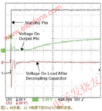

Figures 1 and 2 are graphs depicting typical noise noise. An evaluation board (EVM) from Texas Instruments is used here, with a load of 4W and a power supply voltage of 12V. Note that the shape of the output trajectory before and after the output decoupling capacitor, the sharp transient (sharp transient) are the same. In addition, note that the DC level of track 2 drops to 0V in 40-50 ms before slowly rising to the midrail. Figure 2 shows more detailed information when the device enters the working state from the standby state, but does not indicate the time required for the DC voltage to reach the appropriate bias level.
How does input offset cause transient noise?
Regardless of the supply voltage, the TPA1517's DC bias rating during the input phase is 2.1 V. When the TPA1517 is placed in standby mode, the input bias voltage will drop by a few hundred millivolts or more. When the device returns to working state, the input bias will quickly return to its rated value of 2.1 V. The greater the gap between the input bias voltage in standby and 2.1 V, the greater the instantaneous noise generated when returning to working state. Figure 3 graphically describes the input noise in a 12 V, 4W system. Trace 1 is the voltage on the "STANDBY" pin. Trace 2 is the voltage of the output decoupling capacitor (DC coupling) in terms of load.


How does the output offset cause transient noise?
The rated DC bias of the TPA1517 output stage is VCC / 2. After this setting, the output signal can have a higher output amplitude in the positive direction and the negative direction, and it will not happen that one side is limited by the other side. Unlike many other TI audio power amplifiers, when the TPA1517 is placed in standby mode, the output is not grounded, but in the position of the DC intermediate rail. However, during the transition from standby to working state, the output will show a short but significant instantaneous rise in DC voltage. These voltage spikes (the size of which may reach several volts) are transmitted to the loudspeaker, producing extremely instantaneous noise. The reason for this is that the voltage changes too fast, so that the DC blocking capacitor cannot recognize that this is a change in DC current, so the signal is allowed to pass.
Figure 4 is a capture diagram describing the instantaneous noise caused by the output bias in a 12 V, 4 W system. Note that there is a large voltage surge of nearly 5V on tracks 2 and 3.
Reduce instantaneous noise
The transient noise is caused by the DC bias problem at the input and output stages of TPA1517. In order to reduce the noise as much as possible, it is necessary to find a solution that can solve the problem of input and output offset. This is basically equivalent to two separate solutions, because either solution can be used alone.
Squelch during input
The noise problem caused by the DC input offset problem is not as large as the output offset, but it is more complicated by comparison, so the input offset problem is discussed here first.
Because the noise generated by the input DC bias is caused by the apparent decrease of the input DC bias when the device enters standby mode, it is obvious that a solution is to force the input to be maintained at 2.1 V when the device is in any state.
This solution is not as simple as it looks at first glance. Simply adding a resistor divider to the input circuit to obtain a 2.1 V bias from the power supply is not a good solution. Although it provides the required constant DC bias, it also requires two resistors to be permanently installed on the device side of the input capacitor. Its effect is to greatly weaken the input signal.
We need such a solution: when the device is in standby mode, an external source biases the input, but when the device is in normal operation, the external source will be disconnected. In order to achieve this, a series of switches must be used in conjunction with a resistor divider (the size of which should be suitable for the supply voltage). The first switch is connected to the "STANDBY" pin and functions as an inverter. The second switch is responsible for connecting or disconnecting the 2.1V voltage formed by the "INPUT" pin and the resistor divider.
The input bias current of the TPA1517 is relatively large, so it is necessary to use a resistor with a small impedance value in the resistor divider. This minimizes the effect of input bias current on the 2.1V voltage generated by the voltage divider. It is unwise to use a resistor with a total value in series exceeding 10kΩ because the input bias current will be large enough to significantly change the voltage divider voltage. However, if the resistance value is too low, the current through the resistance will be high, which will generate unnecessary heat. For example, if R1 is 1 kΩ, it will consume approximately 100 mW, R2 will consume approximately 25 mW, and the voltage divider current is 9.84 mA. If the R1 resistance value is reduced from 1kΩ to 100Ω, the voltage divider current at 12 V will jump from 9.84 mA to 98.4 mA. This means that R1 and R2 will consume approximately 1W and 1 / 4W of power, respectively! Refer to Table 1 for the recommended resistance value of the input voltage divider. When choosing resistors, care should be taken to choose resistors with appropriate power ratings.
Squelch at output stage
The effect of the output instantaneous value on the noise is very large. As shown in Figure 2, the output stage is the cause of the largest voltage surge, and this is directly related to the noise that can be heard by the ear.
The solution to the noise caused by the output stage is to quickly (but not immediately) ground the output when the device enters standby mode, and then allow the output value to return to the middle rail when the device returns to operating mode.
If the output is intentionally grounded, the output value will not fluctuate when the device begins to return to operating mode. The output value returns to an appropriate level, and the speaker can only be driven when the output switch is turned off (transistors Q2 and Q3 are output switches, see Figure 5).
Consider input and output squelch together
There must be appropriate circuits around the input and output to obtain the best noise solution. In addition, since the TPA1517 is a stereo amplifier, the noise suppression circuit must be modified so that it can function on both channels with a minimum number of components. To achieve this, only one inverter can be used to drive the input switches on the left and right sides and the output switches on the left and right sides.
Figure 5 is a detailed illustration of a comprehensive stereo solution. The circuit described in Figure 5 uses bipolar transistors, which are generally cheaper than FETs. If you prefer FETs, Figure 6 depicts a similar circuit. "Standby control" should be pulled to the lowest level, this can ensure that changes in VBE will not accidentally activate the circuit.

Audio performance
The TPA1517 transient noise solution described in this article does not increase the total harmonic distortion and noise (THD + N) of the entire system. Figures 7 and 8 contain the results of two THD + N scans with TPA1517 EVM. Figure 7 is a comparison of a THD + N scan and output power scan, and Figure 8 is a comparison of a THD + N scan and frequency scan. The higher distortion at lower frequencies in Figure 8 is caused by the high-pass filter formed by the input capacitor and input resistance.

Reduction of instantaneous noise at power-on and power-off
The noise reduction scheme introduced in this application can also be used to mitigate the effects of power-on and power-off sequencing.
In normal operation, TPA1517 often suffers from large noise during power-on and power-off. Noise suppression circuit can be used to solve this problem. The noise suppression circuit alone cannot play a large role when power is turned off, because the power supply has been eliminated from the noise suppression circuit and the device. However, TPA1517 can be powered on and off in standby mode. When the power-on operation gives the noise suppression circuit enough time to apply the appropriate bias, the TPA1517 is kept in standby mode, so that when the device is placed in operation, the noise can be greatly reduced. Similarly, the noise suppression circuit keeps the output grounded in standby mode, so that when the device is powered off, it is virtually free of noise. Welcome to reprint, this article comes from the electronic enthusiast network (http: //)
Led Lighting,Aluminum Material Reflector,Anodized Parabolic Reflector,Parabolic Grow Light Reflector
Yangzhou Huadong Can Illuminations Mould Manufactory Co., Ltd. , https://www.light-reflectors.com