Low-voltage driven RF MEMS switch design and simulation
In recent years, RF microelectronic system (RF MEMS) devices have attracted wide attention due to their small size and low power consumption. Especially the phase shifters and antennas constructed by MEMS switches are the key technologies for implementing tens of thousands of unit phased array radars. Military is of great significance. In the field of communication, it is also applied to mobile phones with the advantages of ultra-low loss, high isolation and low cost. However, RF MEMS switches generally have problems of high driving voltage and long switching time, which are inferior to FET FET switches and PIN diode switches. Domestic research is still in its infancy relative to the results already achieved abroad. Some improvements will be made below for the MEMS switch defects.
1 General considerations for RF MEMS switches
When the beam or film of the MEMS switch is attracted downward by electrostatic force to reach a certain level, the beam or film is rapidly shifted to the lower plate, and the voltage depends on material parameters, switch size and structure. The material of the beam or membrane needs better Young's modulus and yield strength. The larger the Young's modulus is, the higher the resonance frequency is, which ensures the high speed stability and the switch life of the work; the size effect of the electrostatic driving force should be considered in the dimension design; The natural vibration frequency of the structure affects the maximum operating speed of the switch. From the structural point of view, the way to reduce the driving voltage is: reduce the plate spacing; increase the driving area; reduce the elastic coefficient of the beam or film. Common structures include series and parallel cantilever beam switches, torsion arm switches and capacitive switches. The first three are resistance contact type. There are many problems such as large insertion loss when the metal is in contact with the signal line, and the insulation of the capacitive contact switch. There is also a problem with the media being broken down. Studies have shown that the higher the applied voltage, the shorter the life of the switch, and the lowering of the driving voltage will inevitably lead to a slower switching speed. How to meet the driving voltage and switching speed requirements at the same time is the current difficulty.
2 Simulation and optimization of RF MEMS switches
For a capacitive switch, the driving voltage decreases as the length of the bridge film increases, and the larger the residual stress of the bridge film, the larger the driving voltage. Usually, the Young's tensor is 78 GPa and the Poisson's ratio is O. As the bridge film material of 44, in order to obtain good isolation, the switch has a large permittivity. Here, S3N4 with a dielectric constant of 7.5 is selected as the dielectric layer, and the bridge unit is Solid98, with a voltage of 5 V, and the dielectric is Air, lower plate plus OV voltage. Then use ANSYS to model, mesh, load and solve electrostatic coupling and modal analysis. The switch deformation at 5 V is about O. About 2 μm, the low voltage drive requirement is not yet reached. The first five modes of the extraction switch are shown in Figure 1.
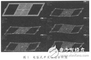
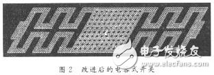
It can be seen that the resonant frequency of the switch from lower order to higher order is larger and larger, 79.9 kHz, 130.3 kHz, 258.8 kHz, 360.7 kHz, 505.6 kHz, and the first-order mode is far away from other modes. State, that is, it is not easy to be disturbed by the outside world, and only the resonant frequency whose control switching frequency is lower than the first-order mode can ensure its stable operation. Since the actual switching time is still not ideal, holes are drilled in the film to reduce the damping of the compression mode, thereby increasing the switching speed. Although the capacitance ratio of the off state is reduced, the hole can reduce the weight of the beam and obtain a higher mechanical resonance frequency. In the final model, a total of 100 holes were dug, and the two ends were bent to reduce the driving voltage. The simulation obtained a capacitive switch with a switching time of 5 μs or less and a stable switching time of 5 μs or less at 5 V, as shown in Fig. 2. Show.
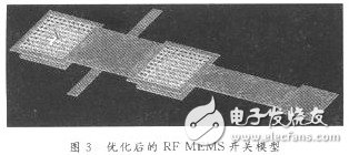
Considering the dielectric breakdown problem still existing in the capacitive switch, the structure is improved here, and the torsion arm lever is combined with the punched capacitor film to reduce the driving voltage and increase the switching speed without affecting the capacitance ratio. Electrical breakdown is suppressed to some extent. The working principle is as follows: when the push electrode is applied with voltage, the lever is lifted up, and the distance between the dielectric film and the contact film is increased, so that the coupling capacitance is small, and the signal passes through the transmission line; when the pull electrode is applied with voltage, the lever is pulled down, the coupling capacitance becomes large, and the microwave signal is reflection. The material selection is still dominated by Au and S3N4, and some parts can be replaced by A1. The structure and size are estimated by the equation of the equation of the transcendental equation and the on-off of the switch. The lower plate is 25 & TImes; 25 (the unit system uses μMKSV, the length unit is μm, the same below), and the insulating dielectric layer is attached. The hole is 3.4 & TImes; 3.4, the lever is 100x30, the structural layer is 20 & TImes; 20, the plate thickness is 1. The results shown in Figure 3 were obtained by ANSYS simulation.
After ANSYS is used for electrostatic coupling and modal analysis, the 3D electromagnetic field simulation of the switch is performed by ANSOFT HFSS, and the insertion loss and isolation are further determined to determine the structure of the coplanar waveguide and the contact film, thereby improving the RF performance of the switch. In the modeling, the bending of the switch is ignored, the material characteristics and the air radiation boundary are defined, and the wave port port is used for simulation to solve the isolation of the open state and the isolation of the off state. When the dielectric layer is thin, the switch has good isolation around 10 GHz and the insertion loss is below 1 dB.
3 RF MEMS switch preparation process
The rational selection of the process of growing the dielectric film has a great influence on the switching performance. The RF MEMS switch in this paper needs to grow a silicon nitride film on the surface of the substrate. Generally, the LP-CVD process is selected, and the dielectric film is preferably PECVD. The performance requirements of the film are relatively low, and the sputtering method can be used. Considering that the substrate requires leakage current and loss as small as possible, high-resistance silicon and silicon dioxide are used as the substrate, and the latter ensures the insulation requirements. The gold signal line and the lower plate are formed by peeling off the positive gel, and the electron beam is evaporated to obtain an aluminum upper plate. However, from the feasibility consideration, the process realization of some schemes is still difficult for the domestic processing technology, and the performance of the microsystem can only be sacrificed to achieve the processing conditions.
4 Conclusion
This paper mainly innovates from the structure, and obtains the theoretical solution through computer-aided design simulation analysis. It satisfies the original intention of the design to some extent, but it is still immature in the process. Lower driving voltage and higher switching frequency are still urgent problems to be solved. In addition, how to ensure the reliability and practicability of actual products is also the focus of future research.
LED outdoor lighting provides aesthetic
beauty and utility to architecture. It light building, pathways, walls, garden,
fountain, etc. almost anything outdoors you want to illuminate. Our high
quality fixtures come in variety of finishes, sizes and styles to reflect
project requirement.
LED outdoor lights are either a wide voltage AC85-265V system or low voltage
12V/24V system. Of course wide voltage is very convenient for installation and
use. Low voltage systems require a transformer or power supply which converts
the high voltage to 12V/24V. It has advantages allowing the lighting fixtures
to be smaller in size and is safer round people and pets.
Our LED outdoor lighting technology and quality control system will bring the
outdoor illumination solution perfectly and make the project more economical in
its operation.
LED outdoor lighting cover kinds of category, there are Led Flood Light, street
light, High Bay Light, wall washer light, underground light, underwater light,
spike light, wall light, step light, Digital Tube light, point light, strip
light and other Decoration Lighting.
We are manufacturer, not only product we care, but also lighting solution. You
will get suitable advice.
Led Outdoor Light,Led Flood Light,Led High Bay Light,Led Street Light
ZHONGSHAN G-LIGHTS LIGHTING CO., LTD. , https://www.glightsled.com