High frequency pcb interference problem and solution
In the actual research, we conclude that there are four main types of interference, including power supply noise, transmission line interference, coupling, and electromagnetic interference (EMI). By analyzing various interference problems of high-frequency PCBs, combined with practice in practice, an effective solution is proposed.
First, the power supply noiseIn high-frequency circuits, the noise of the power supply is particularly significant for high-frequency signals. Therefore, the power supply is first required to be low noise. Here, clean ground and clean power are just as important, why? The power supply characteristics are shown in Figure 1. Obviously, the power supply has a certain impedance, and the impedance is distributed over the entire power supply, so the noise is also superimposed on the power supply. Then we should reduce the impedance of the power supply as much as possible, so it is best to have a proprietary power plane and ground plane. In high-frequency circuit design, the power supply is designed in layers, which is much better in most cases than in the form of a bus, so that the loop can always follow the path with the least impedance. In addition, the power board has to provide a signal loop for all generated and received signals on the PCB, which minimizes the signal loop and reduces noise, which is often overlooked by low-frequency circuit designers.
There are several ways to eliminate power supply noise in PCB design.
1. Pay attention to the through hole on the board: the through hole makes it necessary to etch the opening on the power supply layer to leave space for the through hole to pass. If the power supply layer is too large, it will affect the signal loop, the signal will be forced to bypass, the loop area will increase, and the noise will increase. At the same time, if some signal lines are concentrated near the opening, sharing this loop, the common impedance will cause crosstalk.
2. The connection line needs enough ground wire: each signal needs its own proprietary signal loop, and the loop area of ​​the signal and loop is as small as possible, that is, the signal and the loop are parallel.
3. The analog and digital power supplies should be separated: high-frequency devices are generally very sensitive to digital noise, so the two should be separated and connected together at the entrance of the power supply. If the signal crosses both analog and digital, the signal can be Place a loop across the span to reduce the loop area.
4. Avoid separate power supplies that overlap between different layers: otherwise circuit noise is easily coupled through parasitic capacitance.
5. Isolation of sensitive components: such as PLL.
6. Place the power cable: To reduce the signal loop, reduce the noise by placing the power cable on the side of the signal line.
Second, the transmission line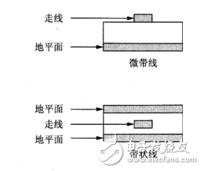
There are only two kinds of transmission lines in the PCB: strip line and microwave line. The biggest problem of the transmission line is reflection. The reflection will cause many problems. For example, the load signal will be the superposition of the original signal and the echo signal, which will increase the difficulty of signal analysis. Reflection can cause return loss (return loss), and its effect on the signal is as severe as the effect of additive noise interference:
1. Signal reflection back to the signal source will increase system noise, making it more difficult for the receiver to distinguish noise from signal;
2. Any reflected signal will basically reduce the signal quality, which will change the shape of the input signal. In principle, the solution is mainly impedance matching (for example, the interconnection impedance should match the impedance of the system), but sometimes the calculation of the impedance is cumbersome. You can refer to some calculation software for transmission line impedance.
The method to eliminate transmission line interference in PCB design is as follows:
(a) Avoid impedance discontinuities in the transmission line. The point at which the impedance is discontinuous is the point at which the transmission line is abrupt, such as a straight corner, a via, etc., and should be avoided as much as possible. The method is as follows: avoid straight corners of the traces, as far as possible to take a 45° angle or an arc, and a large corner can also be used; use via holes as little as possible, because each via is a discontinuous point of impedance, and the outer layer signal is avoided. The inner layer and vice versa.
(b) Do not use pile lines. Because any pile line is a source of noise. If the pile line is short, it can be terminated at the end of the transmission line; if the pile line is long, the main transmission line will be the source, which will cause a large reflection, which complicates the problem and is not recommended.
Third, coupling1. Common impedance coupling: It is a common coupling channel, that is, the interference source and the interfered device often share certain conductors (such as loop power, bus, common ground, etc.).
2. Field common mode coupling will cause the radiation source to cause a common mode voltage on the loop formed by the disturbed circuit and the common reference plane. If the magnetic field is dominant, the value of the common mode voltage generated in the series-connected loop is Vcm=-(ΔB/Δt)* area (where ΔB = the amount of change in magnetic induction). If it is an electromagnetic field, it is known. Its electric field value, its induced voltage: Vcm = (L * h * F * E) / 48, the formula is suitable for L (m) = 150MHz or less, beyond this limit, the calculation of the maximum induced voltage can be simplified as: Vcm = 2*h*E.
3. Differential mode field coupling: Refers to the direct radiation being sensed by the wire pair or the leads on the circuit board and its loop. If you are as close as possible to the two wires. This coupling is greatly reduced, so the two wires can be twisted together to reduce interference.
4. Inter-line coupling (crosstalk) can cause any line to be equal to undesired coupling between parallel circuits, which can seriously impair system performance. Its types can be divided into capacitive crosstalk and inductive crosstalk. The former is because the parasitic capacitance between the lines causes the noise on the noise source to be coupled to the noise receiving line by the injection of current; the latter can be thought of as the coupling of the signal between the primary and secondary of an unwanted parasitic transformer. The magnitude of the inductive crosstalk depends on the proximity of the two loops and the size of the loop area, as well as the impedance of the affected load.
5. Power line coupling: It means that the AC or DC power line is subjected to electromagnetic interference, and the power line transmits these interferences to other devices.
There are several ways to eliminate crosstalk in PCB design:
1. The magnitude of both crosstalk increases as the load impedance increases, so the signal lines sensitive to interference caused by crosstalk should be properly terminated.
2. Increase the distance between signal lines as much as possible, which can effectively reduce capacitive crosstalk. Ground layer management is performed, and the spacing between the wirings is made (for example, the active signal lines and the ground lines are isolated, especially between the signal lines where the state jumps and the ground), and the lead inductance is reduced.
3. Inserting a ground line between adjacent signal lines can also effectively reduce capacitive crosstalk. This ground line needs to be connected to the ground plane every 1/4 wavelength.
4. For inductive crosstalk, the loop area should be minimized and, if allowed, eliminated.
5. Avoid signal sharing loops.
6. Focus on signal integrity: Designers must implement terminations during the soldering process to address signal integrity. Designers using this approach can focus on shielding the microstrip length of the copper foil for good signal integrity. For systems that use dense connectors in the communication structure, the designer can terminate with a single PCB.
Switching Residual Current Transformer
Switching Residual Current Transformer,Switching Transformer,Open Residual Current Transformer,Busbar Open Residual Current Transformer
Zibo Tongyue Electronics Co., Ltd , https://www.tongyueelectron.com