**Single-Ended Flyback Circuit Operation**
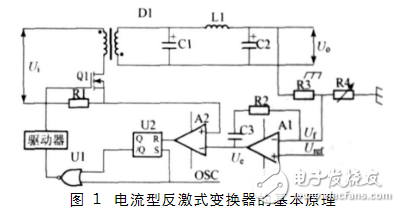
The single-ended flyback switching power supply utilizes a well-stabilized dual-loop feedback system, which includes an isolated output DC voltage sampling feedback loop as the outer loop and a primary coil magnetizing peak current sampling feedback loop as the inner loop. This control system allows the PWM (Pulse Width Modulation) modulator to quickly adjust the pulse duty cycle, effectively regulating both the output voltage from the previous cycle and the peak current in each cycle, ensuring a stable output voltage. A key advantage of this feedback control circuit is its fast dynamic response when there are significant changes in input voltage or load current. It also automatically limits the load current, and its compensation circuit is relatively simple. The flyback topology is particularly suitable for low-power switching power supplies, and its schematic is shown in Figure 1.
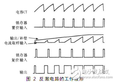
This section provides an analysis of current-mode PWM operation under ideal no-load conditions. Compared to voltage-mode PWM, current-mode PWM introduces an additional inductor current feedback mechanism.
In the diagram: A1 is the error amplifier; A2 is the current detection comparator; U2 is the RS flip-flop; Uf is the feedback sample of the output voltage Uo. The feedback sample is compared with the reference voltage Uref through the error amplifier A1, generating an error signal Ue, which is also compared with the clamping voltage at A2.
When the FET Q1 is turned on, the inductor current iL increases linearly with a slope of Ui/L, where L is the primary inductance of T1. The inductor current is sampled via resistor R1, producing u1 = R1 × iL. This voltage is sent to the current detection comparator. When u1 exceeds Ue, A2 outputs a high level, resetting the RS flip-flop U2. As a result, the NAND gate U1 outputs a low level, turning off Q1. When the clock signal is high, the NOR gate U1 remains low, blocking the PWM. When the oscillator clock falls, both inputs of the NOR gate U1 go low, allowing Q1 to turn on again.
From this analysis, it can be seen that the rising edge of the current-mode PWM signal is determined by the falling edge of the oscillator clock signal, while the falling edge is controlled by the inductor current and the error signal from the error amplifier. Its operational sequence is illustrated in Figure 2.
The single-ended flyback switching power supply operates through periodic on-off cycles of the main switch. When the switch is on, energy is stored in the primary side of the transformer. When it turns off, the transformer transfers the stored energy to the load through the rectifier diode until the next pulse arrives, starting a new cycle.
The pulse transformer plays a crucial role in the switching power supply. It enables the conversion of electrical energy into magnetic energy and back into electrical energy, providing a stable DC voltage for the load. Additionally, it acts as a transformer, allowing multiple DC voltages to be output through different windings to power various circuit components. Lastly, it provides electrical isolation between the hot ground and the cold ground, preventing electric shocks and ensuring user safety.
**Three Working Modes and Output Waveforms of Single-Ended Flyback Circuits**
The flyback power supply operates in three distinct modes: continuous conduction mode (CCM), discontinuous conduction mode (DCM), and critical conduction mode (CrCM).
**(1) Continuous Conduction Mode**
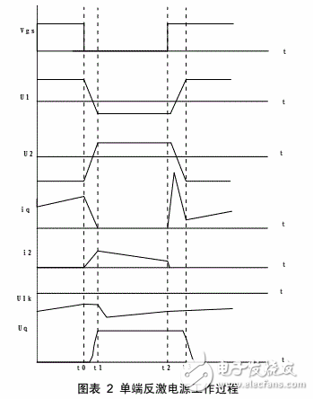
When the single-ended flyback power supply is fully loaded or heavily loaded, the switch duty cycle is large, and the MOSFET remains on before the secondary-side diode turns off. During operation, there is no period where both primary and secondary currents drop to zero, indicating continuous mode. The waveform for this mode is shown in Figure 2.
**Working Process Analysis:**
1) Before time t0, the switch is on, the primary current rises, and the transformer stores energy. The primary voltage is positive, the secondary voltage is negative, and capacitor C1 slowly discharges through R1, causing its voltage to decrease.
2) From t0 to t1, the switch turns off. (a) The primary current decreases rapidly at a rate of Vin/Lm, and the secondary diode turns on, causing the secondary current to rise quickly. (b) The primary voltage drops, while the secondary voltage rises, both crossing zero simultaneously. (c) Due to the junction capacitance of the MOSFET, the voltage cannot change abruptly, resulting in a zero-voltage shutdown. (d) During this phase, the leakage inductance current cannot change abruptly, so C1 begins to charge and starts increasing.
3) From t1 to t2, the primary and secondary voltages, along with the MOSFET voltage, remain largely unchanged. (a) At time t1, U1 reaches its negative maximum, and since its voltage is higher than C1’s, C1 charges quickly to its maximum. (b) As the transformer releases energy, the secondary current gradually decreases.
4) From t2 to t3, the MOSFET turns off. (a) The primary voltage rises rapidly, and the secondary voltage begins to fall, reaching their respective peaks and valleys at time t3. (b) The current has a large peak during this process due to two factors: first, the forced turn-off of the secondary current causes reflection to the primary side, and second, the rapid change in primary inductance voltage leads to a sudden increase in current, reaching a minimum at time t3.
5) After time t3, the MOSFET junction capacitor discharges, and the MOSFET turns on completely, repeating the cycle.
**(2) Discontinuous Conduction Mode**
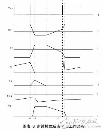
At no load or light load, the flyback power supply may operate in discontinuous mode. In this case, the switch duty cycle is small, and after the switch turns off, the secondary current decreases linearly to zero before the next switch-on event. At this point, both primary and secondary currents are zero, marking the start of the discontinuous mode.
The working process in the intermittent mode is shown in Figure 3.
**Working Process:**
1) The operating state before t0 and t0–t1 is similar to the continuous mode.
2) From t1 to t2, this period can be divided into two parts. (a) The secondary current decreases linearly, releasing the transformer’s stored energy to the secondary side. The primary voltage becomes negative, and the secondary voltage is V2, while the MOSFET voltage drop is (Vin × Np)/Ns. (b) Once the secondary current reaches zero, the primary voltage begins to rise linearly without clamping. Since the current is nearly zero, the voltage change is very slow, and the secondary voltage decreases linearly, while the MOSFET voltage drop also decreases as the primary voltage rises, until the MOSFET turns on at time t2.
3) From t2 to t3, the MOSFET turns on, causing the primary voltage to rise linearly with a slope of Vin/Lm, and the secondary voltage to decrease linearly. The rapid change in primary inductance voltage causes the current to increase rapidly, reaching a minimum at time t3.
4) After time t3, the MOSFET junction capacitor discharges quickly, and the MOSFET turns on completely, repeating the cycle.
**(3) Critical Conduction Mode**
In the critical conduction mode, the operating waveform of the single-ended flyback power supply is shown in Figure 4.
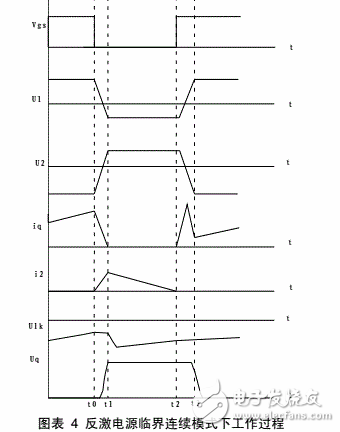
Critical conduction mode represents a transition between continuous and discontinuous modes. It can be analyzed either as continuous or discontinuous mode.
The working process is largely similar to the continuous mode, but with two key differences:
1) At the end of the t1–t2 phase, at time t2, the secondary current drops to zero, and the secondary diode just turns off.
2) The primary current spike in the t2–t3 phase is caused solely by the change in the primary inductor voltage, not by the secondary diode, which aligns more with the behavior seen in the discontinuous mode.
Bang 30000 Puffs
Bang 3000 Puffs Vape
Longhua Manxueling Trading Company , https://www.mxlvape.com