Three solutions for high-side current sensing with wide dynamic range (2)
In many applications such as motor control, solenoid control, communication infrastructure, and power management, current sensing is a critical feature required for precision closed-loop control. How to design a wide dynamic range of high-side current-sense circuits is challenging for most engineers. Here are a few recommended circuits from ADI technologists Neil Zhao, Wenshuai Liao, and Henri Sino for your reference.
Three alternative solutions are presented in order of design complexity from high to low, which provide viable high-accuracy, high-resolution current sensing for a wide range of applications.
1. Construct a current sensor using discrete devices such as op amps, resistors, and Zener diodes. This solution is based on the AD8628 zero-drift amplifier.
2. Use high-voltage bidirectional shunt monitors such as the AD8210 to increase integration and use other external components to extend dynamic range and accuracy.
3. Use device-optimized devices such as the newly introduced AD8217. The AD8217 is an easy-to-use, highly integrated zero-drift current sensor with an input common-mode voltage range of 4.5 V to 80 V.
Solution 2: High-side current sensing with the AD8210 and external devices
Figure 2a shows a simplified block diagram of the integrated high-voltage bidirectional shunt monitor AD8210; Figure 2b shows a unidirectional application with an external reference.
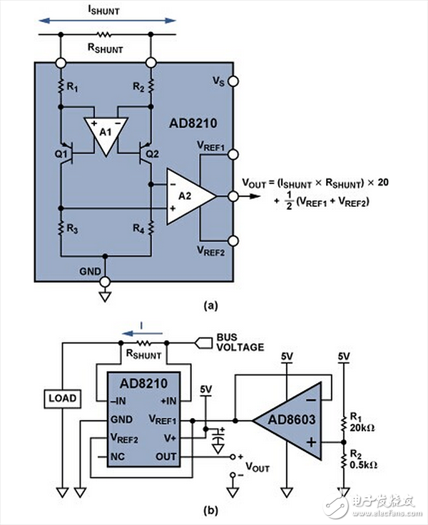
The AD8210 amplifies the small differential input voltage generated by a positive or negative current flowing through the shunt resistor while rejecting high common-mode voltages (up to 65 V) and provides a ground-referenced buffered output.
As shown in Figure 2a, it consists mainly of two modules: a differential amplifier and an instrumentation amplifier. The input is connected to differential amplifier A1 via R1 and R2. A1 uses Q1 and Q2 to adjust the small current flowing through R1 and R2 to zero the voltage at its own input. When the input signal to the AD8210 is 0 V, the currents in R1 and R2 are equal. When the differential signal is non-zero, the current in one resistor increases and the current in the other resistor decreases. The current difference is proportional to the magnitude and polarity of the input signal.
R3 and R4 convert the differential current flowing through Q1 and Q2 into a differential voltage. A2 is configured as an instrumentation amplifier to convert this differential voltage to a single-ended output voltage. The gain is internally set to 20 V/V with a precision-regulated thin film resistor.
The output reference voltage can be easily adjusted using the VREF1 and VREF2 pins. In a typical configuration that handles bidirectional current, VREF1 is connected to VCC and VREF2 is connected to GND. In this case, when the input signal is 0 V, the output is centered at VCC/2. Therefore, for a 5 V supply, the output is centered at 2.5 V. The output will be greater than or less than 2.5 V depending on the direction of current flow across the shunt resistor.
This configuration is ideal for charging/discharging applications, but if the user needs to use the entire output range to measure a unidirectional current, a typical method is to use an external source to set the range, as shown in Figure 2b. At this point, a resistor divider is buffered by an op amp to drive the tied VREF1 and VREF2 pins, causing the output to shift.
When the load current is close to zero, it is difficult to monitor the load current by simply relying on the amplifier. The linear output range of the AD8210 is 50 mV to 4.9 V with a 5 V supply. Assuming a shunt resistor of 10 mΩ in the application, the minimum current flowing through it must be greater than 250 mA to ensure that the output of the AD8210 is above its 50 mV minimum.
The configuration shown in Figure 2b introduces an offset to measure smaller currents. When the amplifier gain is 20 V/V, the relationship between the output voltage and the monitored current can be expressed by Equation 2:
For example, when the resistors R1 and R2 are 9800 Ω and 200 Ω, respectively, the offset voltage is 100 mV. When the differential input is 0 V, the output of the AD8210 is 100 mV and still falls within the linear range. If the shunt current range is 50 mA to 20 A, the input range will be 0.5 mV to 200 mV when RSHUNT = 10 mΩ, and the output range of the AD8210 is 10 mV to 4 V plus the offset voltage, which is 0.11 V to 4.1 V. It is completely within its rated linear range.
In fact, with this configuration, the designer can shift the output of the AD8210 to any point within the power supply range to handle any current range with any asymmetry. Since the precision-regulated resistor is internally connected to the reference input, an op amp is required to buffer the voltage divider. For best results, these inputs should be driven with low impedance. Precision, low-cost op amps that can be used to buffer external references include the AD8541, AD8601, AD8603, AD8605, AD8613, AD8691, and AD8655.
In fact, with this configuration, the designer can shift the output of the AD8210 to any point within the power supply range to handle any current range with any symmetry. Since the precision-tuned resistor is internally connected to the reference input, an op amp is required to buffer the voltage divider. For best results, these inputs should be driven with low impedance. Precision, low-cost op amps that can be used to buffer external references include the AD8541, AD8601, AD8603, AD8605, AD8613, AD8691, and AD8655.
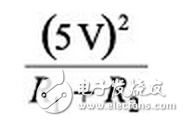
Compared to discrete solutions, this integrated solution requires a shunt monitor with a high common-mode voltage range that requires an output offset when the output voltage range does not meet the current sensing range requirements. But it can handle bidirectional current monitoring and avoids the aforementioned temperature drift and power consumption issues. The guaranteed maximum offset drift drift and gain drift of the AD8210 are 8 μV/°C and 20 ppm/°C, respectively. If the AD8603 is used as a buffer, it contributes an offset of only 1 μV/°C, which is negligible compared to the already low offset voltage drift of the AD8210. The power dissipation of voltage dividers R1 and R2 is:
Calculated with the parameters shown in Figure 2b, the power consumption is only 1.2 mW.
48V Battery Pack ,Switch Battery Pack,Portable Lithium Battery Pack,48V Lithium Ion Battery Pack
Zhejiang Casnovo Materials Co., Ltd. , https://www.casnovonewenergy.com