This article takes a DC/DC step-down power supply chip as an example to explore the internal design of a power management IC. How does it differ from traditional board-level circuit design? One key component inside the chip is the reference voltage, also known as the bandgap reference. This voltage is typically around 1.2V and serves as a stable reference for other internal circuits. The basic principle of a switching power supply involves using a PWM square wave to drive a power MOSFET, enabling efficient voltage conversion.
The internal layout of a motor driver chip, such as the LayOut of a PCB, is visually represented with colors indicating different materials and layers. This visual approach helps in understanding how the chip’s components are arranged internally, similar to how a PCB is laid out.
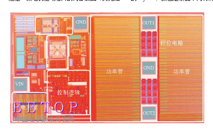
As seen in the image, the internal structure of a chip follows similar principles to those used in PCB design, with clearly defined module layouts. Next, we will examine how the internal circuit diagram of a chip is designed and how it differs from board-level circuit design. Using TI’s popular LM2675 chip as an example, we can look at its block diagram:
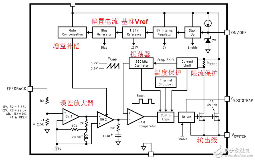
This diagram shows all the internal modules of the power chip. We already know about the BUCK topology. The main function of this chip is to drive the MOSFET and monitor the output state through the FB pin to form a feedback loop that controls the PWM signal driving the power MOSFET, achieving voltage regulation or constant current output. It operates in a non-synchronous mode, meaning the freewheeling diode is external rather than an integrated MOSFET.
Similar to the reference power supply on a board, the internal reference voltage of the chip provides a stable reference for other internal circuits. This reference must be highly precise, stable, and have low temperature drift. The internal reference is called a bandgap reference because its value is close to the bandgap voltage of silicon, which is approximately 1.2V.
Going back to the textbook, the relationship between the current and voltage of a PN junction is exponential. The formula is:
$$ V_{be} = V_T \ln\left(\frac{I_C}{I_S}\right) $$
Where $ I_S $ is the reverse saturation current, proportional to the area of the PN junction. From this, we derive $ V_{be} = V_T \ln\left(\frac{I_C}{I_S}\right) $.
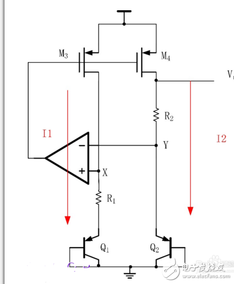
In the circuit, if the op-amp ensures $ V_X = V_Y $, then $ I_1 R_1 + V_{be1} = V_{be2} $, leading to $ I_1 = \frac{\Delta V_{be}}{R_1} $. Since the gate voltages of M3 and M4 are the same, $ I_1 = I_2 $, and thus $ I_1 = I_2 = V_T \ln\left(\frac{N}{R_1}\right) $, where $ N $ is the ratio of the PN junction areas of Q1 and Q2.
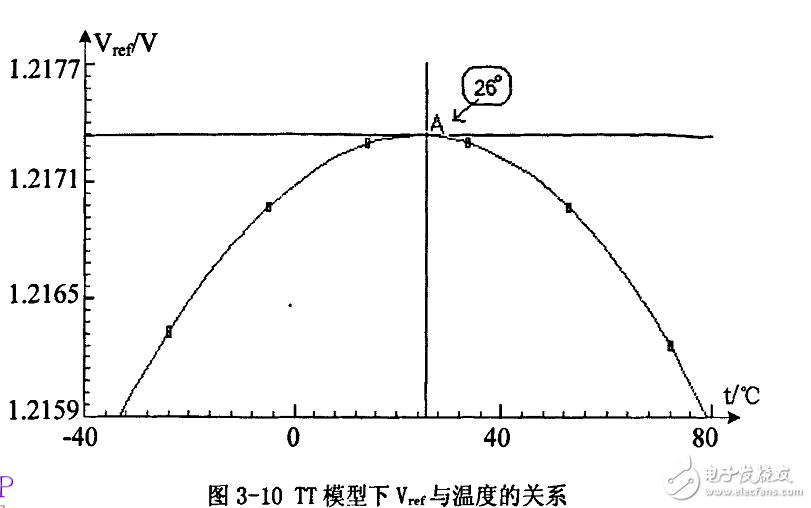
Finally, $ V_{ref} = I_2 R_2 + V_{be2} $. The key here is that $ I_1 $ has a positive temperature coefficient, while $ V_{be} $ has a negative one. By adjusting $ N $, we achieve good temperature compensation, resulting in a stable reference voltage. Typically, $ N $ is set to 8 to achieve zero temperature coefficient. According to the formula, $ V_{ref} = V_{be2} + 7.2 \cdot V_T $, which results in about 1.2V. In low-voltage applications, even lower reference voltages can be achieved, but challenges like power supply ripple suppression (PSRR) remain.
The op-amp design within the chip is critical, as it must maintain high precision and stability across varying conditions. Here's a simplified sketch of the internal design:
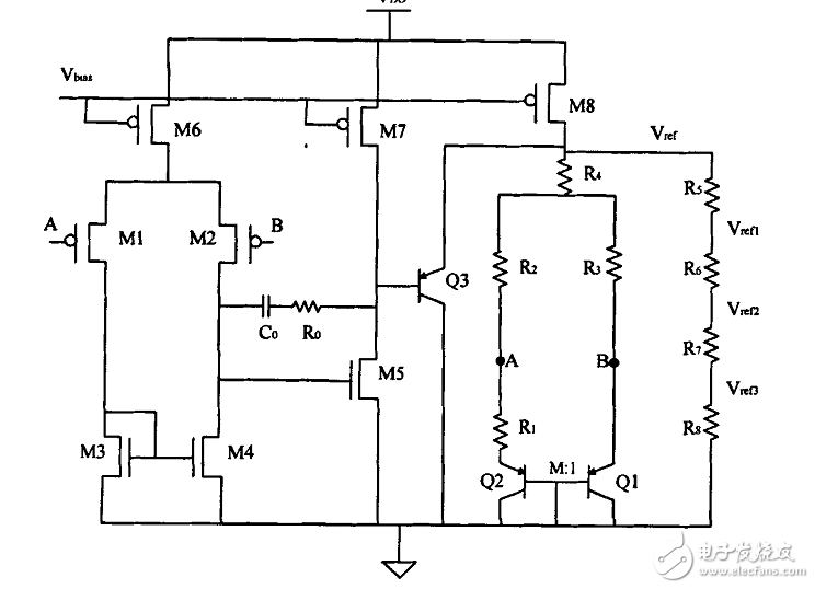
Simulations of the temperature characteristics show how the design compensates for variations, ensuring consistent performance over a wide temperature range.
RC Battery
Rc Battery,New Bright Rc Battery,Rc Battery Pack,Rc Battery Bars
Shenzhen Jentc Technology Co., LTD , https://www.phenyee.com