Design a low-jitter clock high-speed data converter-Design a Low
IntroducTIonMany modern, high-speed, high-performance integrated circuits, such as the MAX104 and MAX106 analog-to-digital converters (ADCs), require a low-phase-noise (low-jitter) clock that operates in the GHz range. Conventional crystal oscillators may provide a low-jitter clock signal, but are not generally available in oscillating frequencies above 120MHz.
Figure 1 illustrates the simplified block diagram of a typical high-speed data converter system. The system consists of a bandpass filter, ADC, high-frequency clock, high-speed storage device, and post processing unit. Aside from the MAX104, the high -frequency clock plays a significant role in determining the accuracy of a high-speed data converter. This high frequency, low-phase-noise clock is a combination of a high frequency voltage-controlled oscillator (U1), a phase-locked loop ( U2), and a crystal oscillator (U3) as shown in Figure 2.
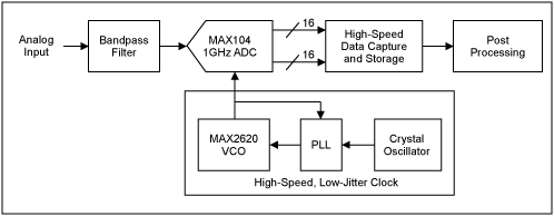
Figure 1. Typical high-speed data converter system using the MAX104 ADC and a PLL-based, low-jitter clock.
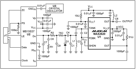
Figure 2. A high-speed, low-phase-noise clock is one of the most critical elements to ensure optimum dynamic performance of the high-speed ADC.
The MAX2620 voltage-controlled oscillator (VCO) is capable of generating oscillator frequencies up to 1GHz, while providing sufficient noise performance. Because of the inherent frequency drift, a phase-locked loop (PLL) is often required to lock the VCO output to the desired frequency by comparing the VCO output to a crystal oscillator frequency.
Choosing an appropriate VCO for a high-speed data converter system is not as simple as finding one with the right oscillator frequency. One key parameter that must be taken into consideration is clock jitter. Jitter is generally defined as short-term, non-cumulative variation of the significant instant of a digital signal from its ideal position in time. Figure 3 illustrates a sampling clock signal that contains jitter. Jitter generated by the clock is caused by various internal noise sources, such as thermal noise, phase noise, and spurious noise. In the case of a data converter, jitter affects the signal-to-noise ratio (SNR) performance of the data converter.
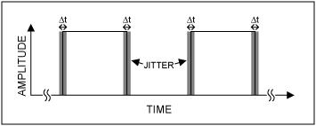
Figure 3. Jitter in clock signal degrades the ADC signal-to-noise ratio.
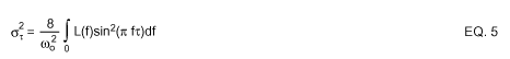
How Clock Jitter Degrades ADC's Signal-to-Noise Ratio (SNR) Jitter generated by a clock source can cause the ADC's internal circuitry to falsely trigger the sampling time. As shown in Figure 4, uncertainty in sampling time Δt equates to uncertainty in amplitude ΔA . This results in false sampling of the analog input amplitude, thus degrading the SNR of the ADC. With the following equations, the maximum SNR of a data converter can be calculated for a given amount of clock jitter:
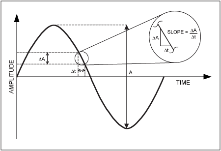
Figure 4. An SNR model obtained using the sampling time uncertainty.
 The slope is at its maximum when the term cos (ωt) = 1. Therefore,
 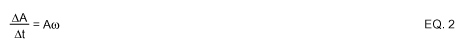 EQ.2 can be rearranged as:
 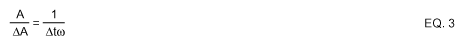 By definition, A / (ΔA) is the signal-to-noise ratio, and Δt is the root-mean-square (RMS) value of the jitter. EQ. ​​3 can be rewritten as:
 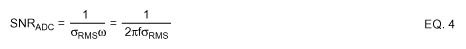 For example, if the analog input signal is 250MHz, and 50dB SNR is to be achieved, the maximum RMS jitter (σRMS) must be less than 2ps. How Noise Sources Cause JitterThermal noise, frequency modulation (FM), amplitude modulation (AM) , phase modulation (PM), and spurious components contribute to the noise that causes jitter in the clock signal. Because of the difficulty to distinguish noise caused by FM, AM, and PM, all three types of noise are grouped into a general term known as phase noise. To clarify the calculation of phase noise, a high frequency circuit, using the MAX2620 VCO and PLL, will be used as example. Thermal Noise Contribution to JitterFigure 5 depicts a simplified plot of the VCO phase noise profile. The MAX2620's output amplifier has a thermal noise floor of approximately -147dBm / Hz. This noise is white, Gaussian noise with a finite bandwidth. Although the effective bandwidth has not been characterized, it can be approximated to be twice the operating frequency. With the MAX2620 properly tuned to the desired output frequency, the contribution of the noise floor to jitter can be computed with the following equation:
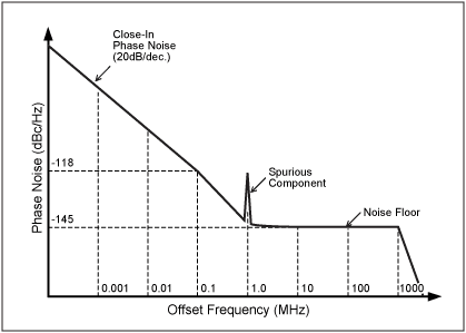
Figure 5. Simplified phase noise profile of the MAX2620 VCO as a function of the offset frequency.
 = Edge-to-Edge Jitter Variance (in s2)
 ωo = 2πfo = Angular clock oscillation (center) frequency (in rad / s)
fo = Oscillator (center) frequency (in Hz)
f = Offset frequency from the center frequency (in Hz)
Ï„ = 1 / 2fo = Half of a period (in s)
L (f) = Phase noise at offset frequency f (in dBc / Hz).
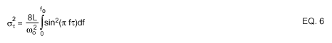
For further improvement in the noise performance, a power matching network (L2 and C6) whose frequency response similar to a bandpass filter is often applied at the VCO output. This attenuates undesired noise outside the bandwidth of interest. By doing so, one can estimate the worst noise by the limit of integration from 0Hz offset to f0. Noise beyond these limits is greatly attenuated and can be ignored. Because the noise floor is even for offset frequencies from 0Hz to f0, L (f) can be considered constant. EQ . 5 can be reduced t
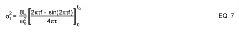
 The edge-to-edge timing jitter due to the noise floor is:
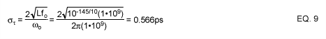
Because thermal noise is non-correlated, jitter is non-accumulated. The period-to-period jitter is the same as edge-to-edge jitter.
Equation 8 can also be displayed as:
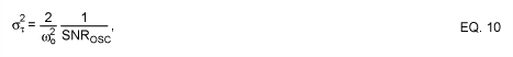 where SNROSC is the signal-to-noise ratio of the oscillator due to the noise floor.
 Phase Noise Contribution to JitterPhase noise is characterized as the ratio of noise power at an offset frequency to the power level of the clock (carrier) signal. This ratio is usually normalized to 1Hz-bandwidth, resulting in a unit of dBc / Hz. For instance, the phase noise at 100kHz offset in Figure 5 is -118dBc. That means the noise power at 1000.1MHz is 118dB below the carrier power level at 1000MHz in 1Hz-bandwidth.
The free running phase noise of the MAX2620 is approximately 20dB / decade from the corner-offset frequency of 1MHz to the clock frequency. With EQ. 11, the period-to-period jitter due the phase noise can be calculated as follows:
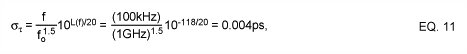 where f is the offset frequency from the clock frequency, and it has to be in the region where the phase noise decreases 20dB per decade. The phase noise, L (f), was taken from the MAX2620 characterization at f = 100kHz offset frequency. With f = 10kHz, the resulting jitter will not change. Spurious Components Contribution to JitterA PLL-based clock signal produces spurs. If these spurs are not suppressed, they can degrade the jitter performance. Figure 6 shows a spectrum plot of a 1GHz clock signal taken with a spectrum analyzer. The two symmetrical pairs of spurs displayed in this figure are approximately 75dBc and 85dBc below the carrier. The separation of these spurs from the carrier and from each other is determined by the comparison frequency used in the phase-locked loop . In this case, the comparison frequency is 1MHz; therefore, the two spurs next to the carrier are exactly 1MHz away from the carrier and the subsequent pair. In addition, there is another pair of -75dBc spurs (no t shown) at 20MHz offset caused by the crystal oscillator. The following equation, translates these spurs into jitter:
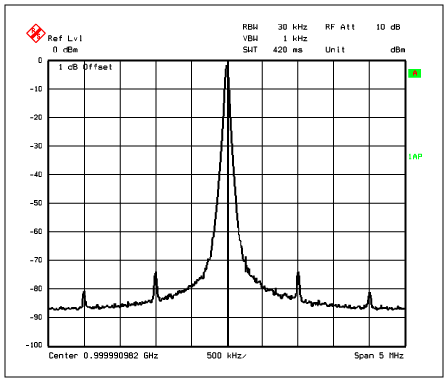
Figure 6. A 1GHz clock shown with spurious components.
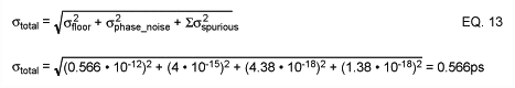
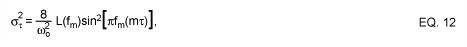 where fm is offset frequency at which the phase noise spurious components occurred. With m = 1, the cycle-to-cycle jitter computes to 4.38x10⁻⁶ps. For practical applications with ADCs, such as the MAX104, jitter due to spurious noise at this level is negligible.
 Total JitterThe total cycle-to-cycle jitter is a function of the square root of the sum of the jitter squares and can be calculated as follows:
 Phase-Locked LoopAs a result of inherit frequency drift due to temperature, power supply, load, etc., a free running VCO is rarely used by itself. Usually a phase-locked loop is introduced to help lock the VCO output to the desired frequency . If designed properly, the phase-locked loop can help reduce the phase noise. The phase noise within the loop bandwidth is lower than that of a free running VCO. Thus, the actual jitter due to phase noise is less than that of EQ. 11.
 Figure 7 shows the functional diagram of the MB15E07 in an integer-N PLL system. It consists of a phase detector (or comparator), an output charge-pump, a dual modulus pre-scalar, an N counter, and an R counter. The N counter consists of a main (M) counter and a swallow or auxiliary (A) counter.
 The N counter then works in conjunction with the dual modulus pre-scalar (P).
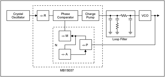
Figure 7. Simplified block diagram of a typical PLL system consisting of a PLL, crystal oscillator, loop filter, and VCO.
During power-up (assuming that the PLL was preprogrammed), the VCO would oscillate at the desired frequency plus some offset. This frequency is first divided by the integer N, and then compared to the reference crystal oscillator frequency, whose frequency has also been divided by an integer R. If there is a phase difference between the two frequencies, the voltage at the PLL output changes accordingly. For example, if the VCO frequency is lower than that of the reference, the charge-pump will charge the loop filter capacitors to increase the voltage. If the VCO frequency is higher than the reference, the charge-pump will discharge the loop filter capacitors to decrease the voltage. An increase in voltage results in an increase in frequency, and visa versa. Hence, the PLL functions as a feedback loop that keeps the VCO output frequency locked at the desired frequency. The VCO frequency is a function of N, R and fREF and is calculated as follows:
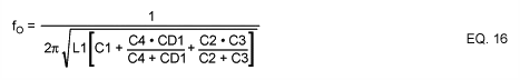
 For example, if P = 32, M = 31, and A = 8, using EQ. 14, N counter is calculated to 1000. If the reference oscillator frequency is 20MHz and the R counter is set for 20, using EQ. 15, the VCO frequency is locked at 1000MHz. Design ParametersCareful design and implementation of the clock circuit is required to ensure optimum performance. This can be achieved by choosing the proper components and providing a well-designed high-frequency PC board. Table 1 shows the recommended component values ​​for two different operating frequencies. These values ​​ensure that the VCO will oscillate and phase lock at the desired frequency, while providing the proper output power levels. The output frequency of the MAX2620 is set by an external resonating tank, which consists of L1 , C1, C2, C3, C4, and D1. L1, C1, C2, C3, and C4 set the free-running, oscillating frequency. The varactor diode, D1, fine-tunes the output frequency to the desired frequency. D1 is reverse biased and has a capacitance that varies with the bias voltage generated by the PLL output. A change in D1's capacitance allows for the fine-tuning of the output frequency.
 The oscillating frequency can be calculated with the following equation:
 To accommodate the component tolerance, PCB, supply voltage, and temperature variations, the capacitance of D1 should be chosen such that the tuning range is about ± 5% to ± 10% from the nominal frequency. C4 is the capacitor that couples the varactor to the tuning tank. Increasing C4 can increase the tuning range. C2 and C3 are feedback capacitors necessary for the oscillator to function properly. Typically, C2 = 2.7pF and C3 = 1.0pF. For 1.0GHz, chose L1 = 5.6nH, C4 = 4.7pF, and C1 = 1.0pF. Both the VCO output and ADC clock input have to be matched to 50Ω. A LC network (L2 and C6) is used at the VCO output to ensure optimum power transfer to the clock input of the ADC . The matching network has a bandpass-filter-like frequency response that further reduces the thermal noise floor.
 Table 1. Suggested Component Values ​​for the Clock Generator
| Designation | Description | ||||
fout = 600MHz | fout = 1000MHz | ||||
| R1 | 240Ω | 390Ω | |||
R2 | 240Ω | 390Ω | |||
C1 | 1.0pF | 1.0pF | |||
C2 | 2.7pF | 2.7pF | |||
C3 | 1.0pF | 1.0pF | |||
C4 | 9.0pF | 3.3pF | |||
C5 | 9.0pF | 2.2pF | |||
C6 | 3.0pF | 1.5pF | |||
C7 | 12nF | 3.9pF | |||
C8 | 120nF | 39nF | |||
C9 | 12nF | 3.9nF | |||
L1 | 12nH (± 2%) | 5.6nH (± 2%) | |||
L2 | 18nH | 10nH | |||
D1 | SMV1233-001 (Alpha Industries) | SMV1233-001 (Alpha Industries) | |||
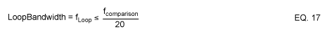
The charge pump output of the PLL pulses at the phase comparison frequency determined by R and the external crystal oscillator. A loop filter is employed to filter these pulses into a constant DC-control voltage for the VCO. The third-order loop filter (Figure 2) consists of C7, C8, C9, R1 and R2. Use simplified EQ. 17 to 23 to calculate the component values.
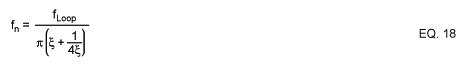
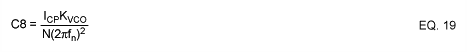

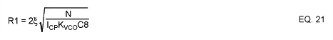

 N = The counter value from EQ. 14
 ξ = Damping factor, typically 0.707
ICP = The charge pump current, 10mA for the MB15E07
KVCO = The VCO tuning gain or sensitivity
The VCO tuning gain, KVCO, depends on the component values ​​used in the VCO tank. The VCO tuning gain in this design example is about 35MHz / V.
The MB15E07 is programmed via the SPI â„¢ -compatible interface. Table 2 shows the register / counter settings for 600MHz (MAX106) and 1000MHz (MAX104) operation:
Table 2. Suggested Register Settings for the MB15E07 with 20MHz Crystal Oscillator
| 600MHz | 1000MHz | ||||
| fCOMPARISON | 500kHz | 1000kHz | |||
Loop Bandwidth | 25kHz | 50kHz | |||
R Counter | 40 | 20 | |||
P Counter | 32 | 32 | |||
M Counter | 37 | 31 | |||
A Counter | 16 | 8 | |||
SW bit | HIGH | HIGH | |||
FC bit | HIGH | HIGH | |||
To ensure good high-frequency PC board layout, keep the following suggestions in mind: Keep all PC board trace lengths as short as possible. Design with controlled impedance traces.
Choose the smallest component size possible, preferably type 0603 or 0402.
Use high quality-factor (Q) components to minimize VCO phase noise and maximize output power transfer. AQ factor of 40 or greater should be sufficient.
Keep all the components for the resonating tank circuit as close together and as close to the MAX2620 as possible.
Place de-coupling capacitors close to the VCO, and with a direct connection to the ground plane. All VCCconnections should have their own de-coupling capacitors.
Maintain a 50Ω connection between the VCO output and the ADC clock input.
Use component value recommendations from Table 1 as a starting point. Possible parasitic effects may require fine-tuning of some component values ​​to ensure optimal performance. Experimental ResultsTo demonstrate the performance of the proposed clock circuit, designed from the suggested equations and techniques, the circuit in Figure 2 was designed and tested with the MAX104 evaluation kit. Figure 6 shows the output of the proposed high-frequency, low jitter clock measured with a spectrum analyzer. The oscillation frequency is phase locked at 1GHz, with an output level of -2dBm . Figure 8 shows the signal-to-noise ratio of the MAX104 ADC over analog input frequency. With fSAMPLE = 1.0GHz and fIN at -1dBFS, the SNR varies from 47.1dB to 45.5dB for analog frequencies ranging from 10MHz to 1GHz, respectively . Compared to a known low-jitter signal generator (HP8662A), the SNR measured with the proposed clock is only ~ 0.4dB lower.
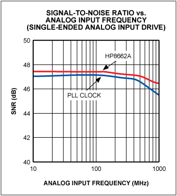
Figure 8. The SNR of the MAX104 is approximately 0.4dB lower with the PLL clock than with the HP8662A.
References: Rudy Van De Plassche, Integrated Analog-To-Digital and Digital-To-Analog Converters, Kluwer Academic Publishers, 1994, pp. 6-8.
Chris O'Connor, "Develop Trimless Voltage-Controlled Oscillators," Microwaves & RF, July 1999 pp. 69-78, and January 2000, pp. 94-105.
Ken Holladay, "Design Loop Filters For PLL Frequency Synthesizers," Microwaves & RF, September 1999, pp. 98-104
MAX2620 Data Sheet, Maxim Integrated Products.
Ali Hajimiri et. Al., "Jitter and Phase Noise in Ring Oscillators," IEEE Journal of Solid-State Circuits, Vol. 34, No. 6, pp. 790-804.
Boris Drakhlis, "Calculate Oscillator Jitter By Using Phase-Noise Analysis," Microwaves & RF, Jan. 2001 pp. 82-90 and p. 157.
MB15E07 Data Sheet. Fujitsu Semiconductor.
MAX104 Data Sheet, Maxim Integrated Products. A similar version of this article appeared in the September 2001 issue of Sensors magazine.
SPI is a trademark of Motorola, Inc.
1"~1.4" speaker (26~36mm)
1) 1" Speaker 26Mm Speaker
2)1.05" Speaker 27Mm Speaker
3)1.1" Speaker 28Mm Speaker
4)1.2" Speaker 30Mm Speaker
5)1.22" speaker 31mm speaker
6)1.25" speaker 32mm speaker
7)1.3" speaker 33mm speaker
8)1.35" speaker 34mm speaker
9)1.4" speaker 36mm speaker


FAQ
Q1. What is the MOQ?
XDEC: 2000pcs for one model.
Q2. What is the delivery lead time?
XDEC: 15 days for normal orders, 10 days for urgent orders.
Q3. What are the payment methods?
XDEC: T/T, PayPal, Western Union, Money Gram.
Q4. Can you offer samples for testing?
XDEC: Yes, we offer free samples.
Q5. How soon can you send samples?
XDEC: We can send samples in 3-5 days.
1" Speaker 26Mm Speaker,1.05" Speaker 27Mm Speaker,1.1" Speaker 28Mm Speaker,1.2" Speaker 30Mm Speaker
Shenzhen Xuanda Electronics Co., Ltd. , https://www.xdecspeaker.com