Design of Digital Video Signal Processing Circuit for LED Full Color Screen
1 Introduction
The LED video display has high brightness, wide viewing angle, long life, high cost performance, and can display various texts, graphics, and images simultaneously with the computer. It can play video signals such as TV, video, and video discs in real time. Multimedia data and other advantages make it widely used in many public places such as streets, squares, commercial centers, sports venues, entertainment venues, and control centers. However, due to technical problems, the large video display still faces severe challenges, mainly manifested in low gray levels, severe loss of brightness, and low refresh rate. In addition, the video signal source in this article comes from the DVI (Digital Video InteRFace) interface. The DVI interface outputs digital video signals with a large amount of information. Generally, it is first buffered by an external RAM (Random Array Memory), and then the video signal is processed by the processor. deal with. There are many types of external memory that can be used for digital image storage, such as SRAM, DRAM, and SDRAM, and their capacities and speeds vary. DRAM and SDRAM are dynamic memories with large capacity and need to be refreshed during use. When the processor does not have an external dynamic RAM interface, it is necessary to design a refresh circuit, which brings inconvenience to system applications; SRAM does not need to be refreshed, does not require a dedicated interface, real-time Good, and can jump addressing, so this article uses SRAM as an external cache memory. The use of sub-field partition storage technology greatly improves the refresh frequency, the image display effect is clear and stable, and achieves a resolution of 800 & TImes; 256, a refresh frequency of 90 Hz, red, green and blue 256 & TImes; 256 & TImes; . At the same time, with this technology, the brightness and gray level are easily adjustable and the brightness loss is small.
2 System composition
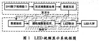
The overall block diagram of the LED video display system is shown in Figure 1: The system consists of two parts: sending and receiving. The function of the sending part is mainly to encode and decode the video signal transmitted by the DVI interface to form 24 b true color video data and dot clock (CLK ), Horizontal synchronization signal (HS), field synchronization signal (VS), data valid signal (DE) and other control signals are transmitted to the receiving card through LVDS (Low Voltage DifferenTIal Signaling) level, and then transmitted to With a specific driving structure (1/8 scanning mode, 74HC595 driving chip) rhythm LED large screen. The focus of this article is to introduce the data processing module of the receiving card.
3 Data processing
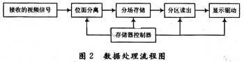
The data processing flow is shown in Figure 2: The receiving card receives the video signal (control signal and data signal) transmitted by the sending card, separates the data in the video signal through the bit plane, stores it in the external buffer in separate fields, and then reads out the partition, Transfer to the display driver screen. The bit-plane separation module reassembles the same weight bits of different data into new data and stores them in the memory. The external buffer adopts the technology of two SRAM ping-pong buffers to realize the pipeline processing of data. The principles and implementation of the bit-plane separation module and sub-field partition storage are introduced below.
3.1 Plane separation module
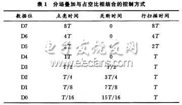
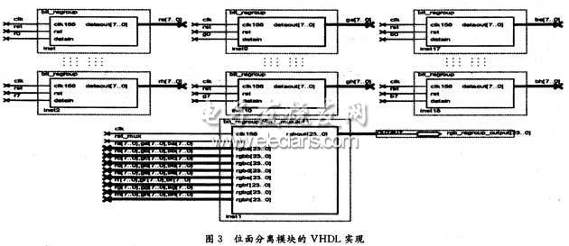
The gray scale control method adopted by the video display screen is a combination of sub-field superposition and duty cycle, as shown in Table 1: where sub-field superposition refers to the use of constant frequency scanning of different fields to achieve different gray levels, such as D7 ~ D4 in Table 1; Duty ratio control refers to controlling the duty ratio of the lighting time and the off time to realize the adjustment of gray scale, such as D3 ~ D0 in Table 1. The premise of these two methods is to achieve the separation of the video data plane. The bit-plane separation is realized by FPGA, which includes two major modules, a data shift register and a data selector. The principle block diagram realized by VHDL is shown in Fig. 3, where r0-7, g0-7 and b0-7 are the red, green and blue colors of the true color image data, each occupying one byte. Register these 24-bit data lines through an 8-bit wide data shift register, and then output them to an external buffer through a color bit selector. The bit-plane separation is realized by controlling the address of the buffer, and the data width of the external buffer is 24 bits, so that the RGB three colors are separated in parallel. Among them, the shift register uses pipeline technology, while latching the output of the same weight bits of the first 8 data, it shifts in the same weight bits of the 9th data, which improves the efficiency of data processing.
3.2 Split field storage
After the data is separated by the bit plane, the same weight bits of different data form new data. By controlling the address of the memory, the same weight bits of all data in a frame are written in the same segment of the memory, so the write address generator requires higher . The system requires 256 levels of gray, so the memory is divided into 8 segments, and each segment stores bits (fields) that represent the same weight. Among them, the 8 segments are replaced by 3 (23) address lines, the large screen with a resolution of 800 * 256 has 256 rows and 800 columns, then the row address is represented by 8 (28) address lines, and these 8 address lines The first 5 bits are the area address (32 areas), and the last 3 bits are the line address of one area (1/8 scan). The column address is represented by 7 (27) address lines. Because the memory is 24 bits wide, one storage unit represents the same weight bits of the 8 RGB points of the LED display, and the order of priority from high to bottom is: field address> column Address> line address. Implemented by counters respectively, the cascade of these three counters constitutes the write address of the memory, and the connection mode is: field address (A17 ~ A15), area address (A14 ~ A10), area line address (A9 ~ A7) Column address (A6 ~ A0). It can be seen that, by changing the priority of the memory address line, sub-field (8 field) storage can be realized.
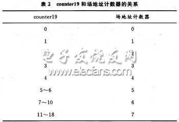
The data is written into the memory in 8 fields, and it needs to be read out in 19 fields when reading, and the display time of each field must be controlled. Therefore, when generating the field address counter of the read address, first design a 19-counter counter 19 (0 ~ 18). Table 2 shows the relationship between counter19 and the field address counter: the display time of each field is implemented with a comparator, and the grayscale and brightness can be flexibly corrected by changing the value in the comparator.
The LED display requires 32 zones to light up at the same time, and uses parallel processing of data to reduce hardware consumption and system operating frequency. Increase the refresh rate. Because the memory can only read one data at a time, it is necessary to use partition latching and then output the 32-area data in parallel.
Row address and column address have the same principle as the write address generator. Here we mainly introduce their priority. The data is already bit-plane separated, so if you want to display the 32 area data at the same time, then the priority of the area address should be the highest, followed by the column address, then the row address, and finally the field address. The connection with the memory is the same as the write address.
Charcoal BBQ Grill,Charcoal Smoker BBQ Grills,Charcoal Barbecue Grill,Charcoal Grill
Shaoxing Haoda Electrical Appliance Co.,Ltd , https://www.hotplates.nl