Implement D/A conversion with IP core in measurement and control system
Abstract: Using digital technology, D/A conversion is realized by IP core in measurement and control system, and realized in one programmable logic device. It is immune to temperature, maintains high resolution, reduces circuit accuracy and stability, and reduces component count.
Keywords: IP D/A VHDL programmable logic device
In all kinds of electronic systems, the proportion of digital circuits is increasing. This is mainly because digital circuits have some outstanding advantages over analog circuits, such as:
* The active device in the digital circuit works in the saturation region and the cut-off region, and the working state is stable;
* Digital circuits process binary signals for easy storage and regeneration;
* Digital circuits are composed of a large number of identical basic units, such as doors, triggers, etc., which are easy to integrate on a large scale and are easy to apply to automated design tools.
Due to the above characteristics of digital circuits, coupled with the rapid development of digital computer and digital signal processing technology, digital circuits have greatly surpassed analog circuits in terms of integration scale, application range and design automation level, and more and more analog circuits The realized functions are transferred to digital circuits and enter the era of digitalization of electronic systems.
In the measurement and control system using digital technology, the D/A originally realized by the analog circuit is realized by the digital circuit. 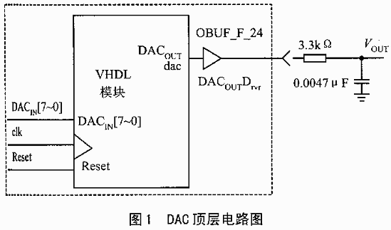
1 IP core introduction
The IP (Intellectual Property) core will be used in digital circuits, but more complex functional blocks, such as FIR filters, SDRAM controllers, PCI interfaces, etc., are designed as modules with modifiable parameters. The reuse of IP cores is the main strategy for designers to win rapid time to market. As CPLDs/FPGAs become larger and more complex, the complexity of ICs increases at a rate of 55% per year, while design capabilities increase by only 21% per year. The designer's main task is to stipulate time. Complete complex designs in the cycle. Calling IP cores can avoid duplication of effort and greatly reduce the burden on engineers, so the use of IP cores is a trend.
IP cores include hard IP and soft IP. Configurable IP is a parameterized retargetable IP with the advantage that functions can be tailored to suit a particular application. These parameters include bus width, memory capacity, enable or disable function blocks.
The biggest advantage of hard IP is to ensure performance, such as speed, power consumption and so on. However, hard IP is difficult to transfer to new processes or integrate into new structures and is not reconfigurable.
Soft IP is delivered in a comprehensive form and must be implemented in the target process and verified by the system designer. The advantage is that the source code is flexible and can be retargeted in a variety of production processes and reconfigured in new functional levels.
However, most libraries are currently charged, but some free IP cores can also be downloaded from the Internet.
2 The function and characteristics of D/A converter realized by IP core
Digital to analog converters (DACs) convert a binary number to a corresponding voltage value. Currently commonly used D/A converters are resistor or capacitor weighted networks, symbol-controlled switches, and reference or current sources. composition. When the D/A converter needs to convert the signal each time the word length is long, the accuracy of these circuits is very high, and the circuit parameters must be kept stable over the entire temperature range and the entire service life. For example, a 16-bit D/A converter whose MSB accuracy must be within 1/2 16 is very difficult. Therefore, there is a need to find a way to maintain high resolution while reducing the accuracy and stability requirements of the circuit.
The synthesizable Delta-Sigma DAC (terminology Delta-Sigma refers to the arithmetic difference sum and Δ-∑ DAC, respectively) is a free IP core provided by Xilinx, which can be downloaded from the Internet.
The Delta-Sigma DAC uses digital technology so it is not temperature sensitive and can be implemented in a single programmable logic device. Avoid using matching resistors in the D/A converter, which is not only cheaper, but also the conversion is linear. The Delta-Sigma DAC is actually a high speed single-bit DAC that uses digital feedback techniques to generate a series of pulses at the output. The time portion of the pulse train that is high is proportional to the binary input, and when the pulse train passes through an analog low-pass filter, an analog output signal is obtained.
Figure 1 is a top-level circuit diagram of a typical programmable logic device implemented with a reset signal, a clock signal, and a binary data bus. The output DACoutDrvr drives an external low-pass filter Vout from 0V to Vcco. Here Vcco is the supply voltage for the FPGA I/O block. The input/output details are listed in Table 1.
Table 1 Input and output description table
| Signal | Direction | Description |
| DACOUT | Output | Drive the pulse train of the external low-pass filter (via an output driver) |
| DACIN | enter | Digital input bus, the value must be set to the positive edge of the clock |
| Clk | enter | Positive edge |
| Reset | enter | Reset signal initializes SigmaLatch and output D flip-flop |
The binary input of the DAC is an unsigned number. “0†represents the lowest voltage and the output analog voltage is only positive. The “0†input produces a 0V output, and the input is all “1â€, then the output is approximately Vcco.
Figure 2 is a block diagram of the Delta-Sigma DAC with the bit width of the binary input being variable. For simplicity, the schematic shows an 8-bit binary input DAC.
In this device, a binary adder is used to generate sums and also to generate differences. Although the input to the Delta Adder is an unsigned number, the outputs of both adders are signed. The Delta Adder calculates the difference between the DAC input and the current DAC output and is represented by a binary number. Because the output of the DAC is a single bit, it is not 1 or 0. As shown in Figure 2, when the input adds 10 digits of the two copies of the output from Sigma Latch to 0, a difference is produced, which also compensates for the fact that DACIN is an unsigned number. The Sigma Adder adds its original output (stored in Sigma Latch) to the output of the current Delta Adder.
The relationship between the output voltage and the input voltage in Figure 1 is
VOUT=(DACIN/(2MSBI+1))&TImes;VCCO
The unit in the formula is V.
For example, for an 8-bit DAC (MSBI=7), the final output is this: the DACIN input is 0, the output is also 0; when the DACI input is hexadecimal FF, the output value is the largest (255/256) & TImes ;Vcco.
The RC low-pass filter is suitable for most applications, and a simple RC low-pass filter works well.
Vs is defined as the absolute value of the change at Vout when the DAC input is increased or decreased. For an 8-bit DAC, Vs is equal to (1/256) & TImes; Vcco.
Vout can generate a variable voltage between 0V and Vcco. The specific value is determined by the bit width of the DACIN and the value entered.
The Delta-Sigma DAC is suitable for low frequency applications that require relatively high precision. In this application, the voltage does not change very quickly, so the time constant of RC can be large to reduce noise.
The most widely used of such DACs is to generate a typical DC voltage. This includes voltage controlled oscillators, voltage controlled operational amplifiers, I/O parameter voltages, programmable voltage sources, waveform generators (sinusoidal, triangular, etc.), reference voltages in A/D conversion, and more.
The Delta-Sigma DAC is an example of how high-speed programmable logic devices can be used in mixed-signal systems to reduce the number of components. The speed and density of programmable logic devices make them ideal components for analog signal generation and processing. 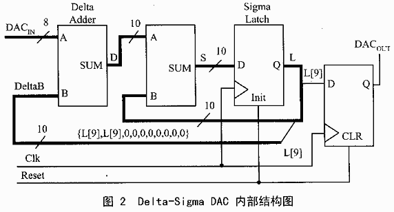
3 Programs written in VHDL
Library ieee;
Use ieeestd_logic_1164.all;
Use ieee.std_logic_arith.all;
Use ieee.std_logic_unsigned.all;
enTIty dac_ds is
Port(reset :in std_logic;
Ck :in std_logic;
Din :in std_logic_vector(7 downto 0);--Signed integer
Dout :out std_logic;
);
End dac_ds;
Architecture arch_dac_ds of dac_ds is
Signal error :std_logic_vector(9 downto 0);--Error accumulator is 2 bits larger
Constant zeros: std_logic_vector(7 downto 0):=(others=>'0');
Begin
Process(reset,clk,din)
Variable val :std_logic_vector(9 downto 0);
Begin
If reset='1'then
Error<=(others=>'0');
Dout<='0';
Elsif clk'event and clk='1' then
--val:=din+error;din is sign extended to nbits+2
Val:=(din(din'high)&din(din'high)&din)+error;
If val(val'high)='0'then
Dout<='1';
Error<=val+("11"& zeros);
Else
Dout<='0';
Error<=val+("01"&zeros);
End if;
End if;
End process;
End arch_dac_ds;
4 chip selection and configuration
The MAX7000S series of programmable logic devices are selected, compiled and automatically configured into the EMP7032SLC44 chip by the MAX+PLUS II software, and the generated object files are programmed through the programming cable.
The D/A converter realized by the IP core is used in the new intelligent resistance furnace temperature controller, because the signal for adjusting the furnace temperature does not require a fast change, so the input binary signal of the DAC is a slowly varying signal. For this low frequency application, the RC time constant can be made larger to reduce noise. In this way, the integrated VHDL language Delta-Sigma DAC module is configured into the EMP7032 chip to achieve the desired results.
Optic Tools And Accessories ,Fiber Optic Equipment ,Optical Fiber,Cable Tools
Optical test instruments,Fiber Optic Equipment Co., Lt d , http://www.nbopticfiber.com