Design and development based on USB data acquisition system
At present, data acquisition cards commonly used in data acquisition systems at home and abroad include RS-232, RS-485 cards, PCI cards, and ISA cards. Although these data acquisition cards have their own advantages, they also have their own shortcomings. For example, the transmission speed of RS-232 and RS-485 cards is slow. The PCI card and ISA card need to be inserted into the PCI slot or ISA slot of the host, which is inconvenient to use. Universal Serial Bus (USB) is a new interface that has the advantages of convenient connection, hot swappable, no external power supply, high transmission speed and low power consumption. USB 2.0 has a maximum transfer rate of up to 480Mbps. Therefore, USB-based data acquisition systems have been widely used in communications, remote sensing, intelligent instrumentation, industrial automation and other fields.
1 system hardware design The hardware part of the data acquisition system is mainly composed of A/D converter AD7829, LPC2132 microprocessor, USB2.0 interface chip ISP1581 and PC. The hardware structure of the USB data acquisition system is shown in Figure 1.
This article refers to the address: http://

Figure 1 system hardware block diagram
The working principle of the data acquisition system: after the signal collected by the sensor is amplified by the modulation circuit, filtered, etc., it enters the AD7829 controlled by the microprocessor for analog-to-digital conversion, and the converted digital quantity enters the microprocessor LPC2132 and temporarily exists therein. Then, the digital interface chip transfers the digital quantity to the PC for data processing, and the control signal sent by the client application of the PC end is transmitted to the data acquisition system with the LPC2132 as the core through the USB interface [1].
1.1 USB interface chip The data acquisition system uses ISP1581 as the USB interface chip. ISP1581 is a cost-effective USB2.0 interface circuit introduced by Philips, supporting 7 IN endpoints, 7 OUT endpoints and a fixed control IN/OUT endpoint. . The ISP1581 supports the self-test mode of SUB2.0 and the return mode of USB1.1, which can run normally under high speed or full speed conditions. It integrates serial interface engine (SIE), PIE, 8KB FIFO memory, data transceiver, PLL 12MHz crystal oscillator and 3.3V voltage regulator. The circuit can be directly connected to ATA/ATAPI peripherals and has a high-speed DMA interface. The transmission rate can be up to 480Mbps/s [2].
1.2 main control chip and A / D conversion chip In order to meet the speed requirements, the main control chip uses LPC2132. The LPC2132 is a Philips ARM7TDMI-STM core-based microcontroller with 64kB of embedded high-speed flash memory and 16kB of on-chip static RAM. Up to 47 5V general purpose I/O ports, one 8-channel 10-bit A/D converter, and a 10-bit D/A converter for different analog outputs. Multiple serial interfaces including two 16C550 industry standard UARTs, two high speed I2C interfaces (400kbit/s), SPITM and SSP. A CPU operating frequency of up to 60 MHz can be achieved with an on-chip PLL [3].
Although the LPC2132 comes with an 8-channel A/D converter, its conversion time per channel is 2.44us, which does not meet the requirements of high-speed data acquisition. Therefore, the AD7829 analog-to-digital converter is used. The AD7829 is an 8-channel 8-bit analog-to-digital converter with a maximum conversion rate of 2Mbps to meet system design requirements.
1.3 hardware interface circuit The hardware connection diagram of the data acquisition system is shown in Figure 2.
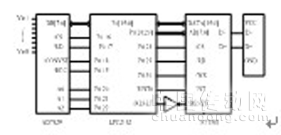
Figure 2 hardware connection diagram
The analog signal is converted into digital by AD7829. The data is first stored in the register of LPC2132, and then the data is transmitted to ISP1581 by LPC2132. Here, the buffer of ISP1581 is defined as 8 and 8 converted data are respectively written. . The PC is connected to the ISP1581 through the USB interface. The ISP1581 is responsible for classifying and interpreting the signals sent by the PC. The specific operation flow is as follows: the data sent by the PC to the USB device is written into the cache of the ISP1581 in the form of a packet, when the cache is written. After the full or data transmission is completed, the ISP1581 sends an interrupt signal to the LPC2132, and the LPC2132 responds to the interrupt signal and enters the interrupt service routine to perform the corresponding packet processing. The USB device cannot actively send data to the host. Only when the PC requires the USB device to send data, the LPC2132 writes the data required by the host to the cache of the corresponding endpoint of the ISP1581 [4].
2 system software design The software part of this data acquisition system mainly consists of three parts: firmware programming, application programming and USB driver design.
2.1 Firmware Programming The conversion pulse/CONVST of the AD7829 is issued by the P0.18 port of the LPC2132. When the AD7829 conversion is completed, the output is active low. After the LPC2132 receives the active level, it sends the next address (via A0, A1, A2 high and low level configuration) to the AD7829, then read the data, when the /78 and /CS signals of the AD7829 are valid, the data is read into the data buffer of the LPC2132 while the next address is hit, so that the loop acquisition 8 analog inputs until the end of data acquisition.
The communication between LPC2132 and ISP1581 is implemented by LPC2132 sending commands and data to ISP1581. The INT interrupt signal of the ISP1581 is connected to the EINT0 port of the microcontroller LPC2132. When the data is successfully received or transmitted, an interrupt is generated. The firmware program responds to these interrupts and completes the configuration of the device. The device firmware program is written in Keil C, including the main loop program, interrupt service program, USB standard request processing and bulk data transfer request processing. As shown in Figure 3.

Figure 3 firmware block diagram
2.2 Application Design Applications include Win32DLL programs and user applications. The Win32 Dynamic Link Library is a binary file containing a shared function library that can be used by multiple applications at the same time. The client application is a software program that implements the functions of the data acquisition system, and is written in Visual C++ in this system.
2.3 USB System Driver Design The USB system driver uses a hierarchical structure model, as shown in Figure 4. Use Windows DDK, a Windows driver development tool provided by Microsoft.

Figure 4 USB layered driver model
The application communicates with the root hub driver through a Win32 subsystem using a Windows-defined software interface (API). The USB root hub driver communicates with the Universal Serial Bus Driver (USBD) via USBDI (Universal Serial Bus Driver Interface). The US2BD then selects one of two host controller drivers to communicate with the host controller below it. Finally, the main controller driver directly accesses the USB physical bus. Before USB is available, it must be configured and interface selected, and then the individual pipes of the selected interface are available. Programming on the basis of USBDI will be greatly simplified. The user does not need to care about the type of IRP, but only needs to construct the USB block in the corresponding distribution routine and send it through USBDI to control the USB device [5] ].
3 Conclusion
The USB data acquisition system is superior to the traditional real-time data acquisition system. It has the advantages of convenient installation, support for plug and play, easy expansion, low electromagnetic interference and high cost performance. The system uses ARM7 chip LPC2132 and USB 2.0 interface control chip ISP1581 to realize the software and hardware design and development of data acquisition system. In the experimental test, the signal generator is used to generate 8 analog signals and connected to the input end of the data acquisition system. The corresponding 8 analog signal waveforms can be displayed on the PC, and the single sampling rate is 150 kSPS. The design requirements prove the correctness and practicability of the design.
References [1] Wang Liping, Wu Liming. Based on the design and development of embedded USB data acquisition system [J]. Electronic Measurement Technology, 2007, 30 (9): 24~26
[2] ISP1581 Users Manual [Z]. Philips Corp
[3] Zhou Ligong, Zhang Hua. In-depth explanation of ARM7[M]. Beijing: Beijing Aerospace University Press, 2005.52~53.
[4] Zhang Guangli, Yan Youyun. Design of USB data acquisition system based on AT89S52 [J]. Instrumentation user, 2008, 03: 33~35.
[5] Zhou Chong, Liu Zhen. Design of USB data acquisition system based on AT89S52 [J]. Science and Technology and Engineering, 2007, 7(22): 5935~5938
Pigtail Cable,Flat Fiber Ribbon Cable,Indoor Ribbon Cable,Indoor Optical Fiber Cable
Shandong Qingguo Optical Fiber Co., Ltd. , http://www.qgfiber.com