Design of PCI ExPress Real-Time Video Acquisition System
Video capture systems are widely used in the industrial field. With the rapid development of multimedia technology, the requirements for video acquisition, processing and transmission performance are also constantly improved, such as high acquisition speed, low power consumption, anti-interference, real-time and scalability. . This paper proposes a multi-functional video processing system with Virtex-5 as the core, ADV7188 as the video decoder and PCIExpress as the transmission bus. The system enables real-time mass transfer of multiple digital video. The PCI Express x1 channel supported by Virtex-6 has a transfer rate of 3.2Gb/s.
Because the system is small in design, low in power consumption and meets the requirements of working conditions, it can be used in public places, factories and underground operations, and requires more remote monitoring environment in harsh places.
1 Introduction to PCI Express Bus
PCI Express is a mainstream serial standard. It was the third generation I/O interconnect technology introduced in 2002, providing an upgrade path from PCI to PCIX. PCI Express is a standard interconnect technology for the PC industry with scalable capabilities, a scalable feature set, strong market adaptability and low cost. Its high-speed serial standard enables bidirectional communication at 2.5 Gb/s line rate per channel, and the hierarchical packet architecture facilitates modular design. Bandwidth enhancements (up to 80 GB) - 1, 2, 4, 8, 16 and 32 channels are achieved with a simpler upgrade. Advanced features of PCI Express, such as reliability, power management, and hot swap, support next-generation 3D/multimedia services with features such as virtual channels, service levels, and quality of service (QoS).
2 system hardware design The system design uses video decoder + FPGA, its function is to receive PAL and other standard analog video signals, converted to meet ITU-R BU. The 656 format digital signal packs multiple channels of video and transmits them to the computer via the PCI Express bus.
Here, the ADV7188 is used to acquire the PAL video signal, and the Videx-5 I2C bus controller is configured and controlled through the I2C bus. Using the XC5-VFX30T from the Virtex-5 series, this device has powerful processing capabilities and a rich interface of external devices to meet the control and image output needs of a variety of different applications. The Virtex-5 device has a video processing IP core that can be configured according to the requirements of the application. It also has IP cores such as PCI Express and PPC440. The PPC440 has a digital processing capability of 1600 DMI/s and a 256 KB SRAM at 667 MHz clock frequency. . Virtex-5 has two I2C interfaces, up to eight (32 bit) peripheral bus interfaces with masters, support for external, internal and inter-memory DMA, 2
10/100/100 Mb/s half or full duplex Ethernet interface, Figure 1 is the hardware block diagram of the system design.
This article refers to the address: http://

3 Principle realization of the main components
3.1 video acquisition processing circuit
3.1.1 Video Decoder Selection When selecting a video decoder, it mainly considers functions, performance, size, cost performance and low power consumption. Therefore, the ADV7188 video decoding device is selected. The device has the following features:
Inputs of NTSC-M/J/4.43, PAL-M/N/B/G/H/I/D and SECAM signals can be detected automatically; single clock 28.636 36 MHz; 4 channels of analog video 12 bits AD acquisition; 5-wire adaptive comb filtering;
Reduced digital noise; integrated automatic gain controller with adaptive white-level peaks; design with weakly locked, noisy and unstable video sources; 12 analog input channels; input video signal amplitude, 0.5 to 1 .5 V; can generate the line sync signal without input video signal; the brightness bandwidth edge enhancement is programmable; the hue, contrast, brightness, saturation are programmable; YCbCr is 20/16/10/8 bit 4 : 2:2 form output; supports industry standard I2C interface; power supply is +3.3 V, 1.8 V; power-down mode; 80-pin, lead-free LQFP package; operating temperature is -40 to +85 °C.
3.1.2 Video Acquisition Circuit Working Principle The video acquisition circuit is based on the ADV7188 as the core, collecting multi-channel PAL, NTSC or SECAM standard analog video signals, with enhanced weak analog video signals, which can be used for noise reduction and digital improvement. The function of video signal quality. The detailed circuit of the AD7188 can be found in the device manual of the ADV7188. Due to the high power requirements of the ADV7188, the system is designed to isolate, decouple, and filter the power supply. For wide application, a quartz crystal resonator with a frequency of 28.636 36 MHz is used here with a frequency difference of ±20 ppm. Figure 2 shows a crystal-mounted crystal oscillator circuit.

According to the PCB layout, Cstray is usually 2 to 3 pF, the capacitance of the ADV7188 device to the power supply is Cpg of 4 pF, and the load capacitance of the quartz crystal resonator is 15 pF. From C1=C2=2(Cload-Cstray)-Cpg, the capacitance values ​​of C1 and C2 can be calculated as 24 pF. According to the preferred value of the E12 series, the capacitance value is 22 pF.
The design uses the power-down mode of the ADV7188. When the film has no analog video input or does not need to work, it will be powered down, and its power consumption will be reduced from 0.6 W to 1 mW during operation, which can greatly reduce system standby. Power consumption.
3.1.3 Configuration of Video Acquisition Circuit The I2C bus controller is designed in the FPGA and configured as an interface bus that is consistent with the video decoder I2C interface clock. Through the FPGA power-on configuration, the FIFO initialization in the FPGA is achieved, and the initialization data is the configuration data of the video acquisition circuit. The configuration data is shown in Table 1.

3.2 FPGA
3.2.1 FPGA device selection
The choice of FPGA model is mainly based on the following aspects: with PCI Express bus; channel is not lower than x8; with embedded microprocessor; suitable I/O pin count and resources, support the required level standard; with lower power Consumption; suitable price/performance ratio.
Therefore, choose Xilinx's Virtex-5 series XC5VFX3-0T, packaged as FF665 PCI Express bus; with PowerPC440 embedded microprocessor. The configuration chip uses a CF card with a capacity of 1 GB.
3.2.2 FPGA performance and resources 1) Clock resources 32 global clock buses, clocking all resources on the entire device, and can drive logic signals;
2) Clock management technology clock de-skew, frequency synthesis, phase shift and dynamic reconfiguration;
3) The phase-locked loop acts as a frequency synthesizer for the broad-spectrum frequency and cooperates with the DCM of the CMT as a jitter filter for the external or internal clock;
4) BLOCK RAM 2 448 Kb, which can be configured as RAM, dual port RAM and FIFO, etc., and its contents can be initialized;
5) configurable logic blocks to implement the main resources of combinational logic and sequential logic;
6) SelectIO resources support a wide variety of standard interfaces. Programmable control including output intensity and slope, and on-chip termination for digitally controlled impedance;
7) SelectIO logic resources include combined input/output, tri-state output control, registered input/output, registered three-state output control, DDR input/output, and DDR output tri-state control;
8) Advanced SelectIO logic resource input string and conversion and output parallel and serial conversion;
9) DSP logic 64 550 MHz DSP48E slices, each DP48E includes a 28x18 multiplier, an adder and an accumulator. The internal structure of the FPGA can also be observed using the FPGA Edit of Xilinx ISE.
3.3 Data Cache Because the bus baud rate of PCI Express is 2.5 Gbps, it is much larger than the digital video signal after 1 channel acquisition. When the video data is transmitted to the FPGA through the parallel bus, the data is buffered by the FIFO configured as the asynchronous input and output, thereby improving the bus use efficiency. If the PCI Express bus is ×1 channel, the PAL video is converted to the commonly used 8-bit 4:2:0 YUV format digital video. According to the PCI Express bus transmission effective data of 1.62 Gb/s, theoretically 36 channels can be transmitted.
3.4 FCI Express interface implementation is designed with FPGA with PCI Express. Xilinx's Virtex-5 LXT series FPGA is used to design with its PCI Express IP core. The functions are as follows: The local link of the user interface is Frame interface; 64-bit data bus width and 3-bit alert bus; packetized interface with frame start (SOF) and end of frame (EOF) for tagged packets; packet interrupt feature for user interface in transmit and receive directions; framing error Detection support; multi-channel configuration support: × 1, × 2, × 4 and × 8; here the channel configuration is × 1; throughput of 1.62 Gb / s or higher per channel; using auto-negotiation in the integrated endpoint module Function that allows the design to use lower bandwidth when certain channels are not working; 8B/10B decoding and decoding used in the physical layer. Although this scheme is difficult to develop and has a long cycle, it has the characteristics of simple external circuit, low hardware cost, flexible design, high integration and easy upgrade. Its interface circuit is shown in Figure 3.

3.5 Clock This design requires 4 clock signals, of which the video decoding signal has the highest clock requirement, the clock precision must be within ±50 ppm, and the clock frequency of the PCI Express bus operation. The DCM and PLL processing of the clock signal in the FPGA completes the functions of de-skewing, phase shifting and frequency synthesis of the clock signal.
3.6 Flash and DDRSDRAM
In order to make the design flexible, scalable and upgradeable, Flash and SDRAM are reserved to store programs and run programs to meet the requirements of intelligence and easy Ethernet remote control.
3.7 Ethernet interface circuit The Ethernet interface circuit is composed of FPGA+PHY+transformer. You can use this interface to load the program. You can also use this interface to connect with the Internet. Using XILINX's FPGA development software ISE, the IP core in the FPGA is used according to the TriMode Ethemet MAC.
3.8 DMA Transfer This design uses DMA for internal data transfer. The digital video signal is transmitted to the FPGA through the parallel bus, and the data is buffered through the FIFO, and transmitted to the computer through the PCI Express through the DMA method.
3.9 FPGA Configuration Scheme The Virtex-5 configuration scheme uses System ACE CF (CompactFlash) in System ACE (System Advandced Configuration Eviroment). The System ACE uses CF memory cards to store data and configures the data into the FPGA through the System ACE controller. System ACE CF uses a 1 GB CompaetFlash card. System ACE CF is a pre-configured configuration solution that requires no programming and requires simple debugging. This solution loads the old version for debugging and the new version into the same CF card, shortens the development cycle, facilitates maintenance and troubleshooting, and saves the application software and the manual attached to the product to the CF card. The system upgrade can replace the CF card, in the system programming and remote upgrade through Internet.
3.10 The power supply design board requires five types of power supplies: +3.3, +2.5, +1.8, and +1.2 V. The +3.3 V power supply is an external input, about 20 W; +1.8 V is provided to the secondary power supply of the FPGA and ADV7188, and the other is the secondary power supply to the FPGA. The +3.3V power supply is the power supply layer, and the +2.5V, +1.8 V, and +1.2V provided to the FPGA are the power layer split. The +1.8V supply current supplied to the ADV7188 is designed to be 0.5A, with a typical typical value of 100 mA. Decoupling capacitors and corresponding components are placed in the same layer to reduce the effects of vias.
3.11 PCB Design PCB layout follows the design requirements for signal integrity. The PCB has a total of 10 layers. Firstly, the power layer and the ground layer are designed. The power layer is 2 layers and the ground plane is 4 layers, which are symmetrically distributed. All the working power supplies except the Ethernet transformer are grounded to ensure the integrity of the ground plane.
Since the PCI Express bus is 2.5Gb/s, when the Virtex-5 pin is allocated, the PCI Express pins are routed as short as possible. In the layout of the PCB, the Virtex-5 is close to the electrical connector of the PCI Express bus interface, and the actual length of the differential pair is no more than 30 mm. During PCB layout, the length difference of differential pairs should be strictly controlled. In order to avoid the delay of signal round trip does not exceed its rise time, overshoot and ringing occur. The PCB layout defines the differential pair length difference not exceeding 1 according to the characteristics of the PCI Express signal. Mm, the actual wiring result does not exceed 0.2 mm. The differential impedance on the PCB is (100 ± 10) Ω, which meets the PCI Express specification's single-ended impedance of (50 ± 10) Ω.
3.12 Operating System The FPGA in this design has a PPC440 core and uses a real-time multitasking operating system (Vxworks). According to the actual use requirements, the task management, communication mechanism, system configuration, and system interface of the Vxworks system kernel (wind) are several. The aspects are designed to ensure the safety and reliability of the system. This design has a mature Vxworks operating system.
3.13 FPGA debugging
FPGA development includes process management and design input, simulation, synthesis, constraint, implementation, place and route, and configuration debugging. FPGA debugging takes up about 80% of the design cycle. Advanced components included with ISE, including ChipScope Pro, PlanAhead, Timing Analyzer, Floor Planner (FloorAhead), Underlay Editor (FPGA Editor), and Power Analyzer (Xpower), along with third-party software ModelSim, effectively uses the tools to speed up the design process, avoid redesign, increase design productivity, and significantly improve design performance, reducing overall power costs.
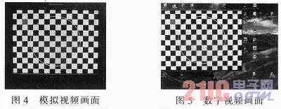
4 Acquisition, transmission and verification An analog video signal generated by the video signal generator is shown in Figure 4. Through the acquisition of the analog video signal and the bus transmission process, the digital video displayed by the computer display is as shown in FIG. 5, and is the same as the analog video image displayed by the monitor, and the naked eye cannot distinguish the difference and meet the use requirements. A variety of standard test pictures of the analog video were collected, showing normal distortion-free, confirming that the video capture and data transmission of the design achieved the desired result.
5 Conclusion With the widespread use of multimedia in industry and commerce, higher requirements are placed on video signal acquisition, data transmission speed, integration and reliability. The PCI Express-based video acquisition system designed in this paper is suitable for collecting weak or interfered video signals with high integration. It is suitable for mass video data transmission and solves the bottleneck problem of transmission.
DITUO Plastic Diffuser has many advantages as below:
- Purifying the air. The Plastic Diffuser generates a large amount of active oxygen anion, which generates a strong reaction with harmful gas molecules in the air, comprehensively removes, and completely eliminates the harm of formaldehyde, benzene and ammonia.
- the use of safety. Plastic Essential Oil Diffuser can produce 100% of the cool mist can maintain the active ingredients of essential oils, so that the essential oils are more easily absorbed by the body to achieve maximum effect; within 2 seconds can feel the original aromatherapy effect. It is fundamentally different from the traditional heating and burning hot fog method. Its cold fog technology does not damage any components of the essential oil, does not cause secondary pollution, and is safer to use.
- small size. Aroma Diffuser water volume of about 100ml, just add 2-3 drops of essential oil in water to achieve aromatherapy.
- strong corrosion resistance. Good Air Diffuser is made of special ABS material, resistant to oil, water and chemical corrosion.
- let the indoor air become fresh. When welcoming guests to visit, or mind the smell in the room, the fragrance of the Scent Diffuser to make the air fresh.
- Concentration. When sitting for a long time or studying alone, let the faint aroma of the Essential Oil Diffuser refreshing.
- Relax before going to bed. When you are busy with your day and want to relax your body and mind, you will feel relaxed and comfortable through the fragrance of the aroma diffuser.
Plastic Diffuser
Plastic Diffuser,Plastic Essential Oil Diffuser,Aroma Diffuser,Air Diffuser
Shenzhen Dituo Electronic Co.,Ltd. , http://www.sz-dituo.com