NVIDIA Denver processor first core photo exposure
 At the 2011 Financial Analyst Conference, NVIDIA chief Huang Renxun not only talked about some behind-the-scenes stories of the ARM architecture processor "Project Denver", but also exposed the kernel photo (or schematic) of the 64-bit processor for the first time. ).
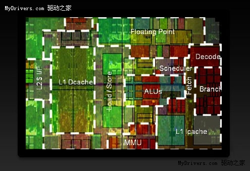
 This at least proves that NVIDIA has already obtained a prototype of a prototype Denver processor and has taken a firm step on its own processor. Of course, since everything is still in development, it is hard to say what the processor is like. At present, the manufacturing process, the kernel area and other parameters have no way of knowing. However, NVIDIA has carefully identified the name and scope of each functional module, so that we have a preliminary understanding of the internal conditions of the Denver processor.
From the figure you can see:
Pickup Unit Decoder Scheduler Arithmetic Logic Unit (ALC)
Floating Point Unit (FPU)
Load and Memory Unit Memory Management Unit (MMU)
Level 1 instruction cache (L1 Icache)
Level 1 Data Cache (L1 Dcache)
The second-level cache logic instruction and the pick-up unit have the largest area of ​​the first-level data cache, and the other-level data cache and the floating-point unit are not small. If the codename Maxwell's NVIDIA next-generation GPU processor uses 512-bit-bit width and high-speed GDDR5 particles, its built-in Denver processor core is expected to have an internal bandwidth of more than 2TB/s and external bandwidth of 320GB/s or more. That is a blockbuster.
Of course, whether the Denver project succeeds is not only because NVIDIA wants to create a truly complete processor chip, but more importantly is whether NVIDIA can establish a complete ecosystem.
Street Lamp Pole
Futao Metal Structural Unit Co., Ltd. , http://www.yxsteelpole.com