Analysis of Thermal Effects of High Frequency PCB Circuits
When the high frequency/microwave RF signal is fed into the PCB circuit, the loss caused by the circuit itself and the circuit material will inevitably generate a certain amount of heat. The greater the loss, the higher the power through the PCB material and the greater the heat generated. When the operating temperature of the circuit exceeds the rated value, the circuit may cause some problems. For example, the typical operating parameter MOT, which is well known in the PCB, is the maximum operating temperature. When the operating temperature exceeds the MOT, the performance and reliability of the PCB circuit will be threatened. Through the combination of electromagnetic modeling and experimental measurement, understanding the thermal characteristics of RF microwave PCBs helps to avoid circuit performance degradation and reliability degradation caused by high temperatures.
Understanding how insertion loss in circuit materials is produced is an important factor in helping to better describe the thermal performance of high-frequency PCB circuits. This article will take the microstrip transmission line circuit as an example to discuss the trade-off factors related to thermal performance of the circuit. In a microstrip circuit with a double-sided PCB structure, losses include dielectric loss, conductor loss, radiation loss, and leakage loss. The difference between the different loss components is large, and with a few exceptions, the leakage loss of the high frequency PCB circuit is generally low. In this paper, since the leakage loss value is very low, it is ignored for the time being.
Radiation loss
Radiation loss depends on many operating parameters such as operating frequency, circuit substrate thickness, PCB dielectric constant (relative dielectric constant or εr) and design scheme. In terms of design, radiation loss often results from poor impedance conversion in the circuit or differences in electromagnetic wave transmission in the circuit. The circuit impedance transformation region typically includes a signal feed region, a step impedance point, a stub, and a matching network. A reasonable circuit design can achieve a smooth impedance transformation, which in turn reduces the radiation loss of the circuit. Of course, it should be realized that there is a possibility that impedance mismatch causes radiation loss at any interface of the circuit. From the point of view of the operating frequency, usually the higher the frequency, the greater the radiation loss of the circuit.
The parameters of the circuit material associated with the radiation loss are mainly the dielectric constant and the thickness of the PCB material. The thicker the circuit substrate, the greater the possibility of radiation loss; the lower the εr of the PCB material, the greater the radiation loss of the circuit. A comprehensive trade-off of material properties, the use of thin circuit substrates can be used as a way to counteract the radiation losses caused by low εr circuit materials. The effect of circuit substrate thickness and εr on circuit radiation loss is due to its frequency dependent function. When the thickness of the circuit substrate does not exceed 20 mils and the operating frequency is lower than 20 GHz, the radiation loss of the circuit is very low. Since most of the circuit modeling and measurement frequencies in this paper are below 20 GHz, the discussion in this paper will ignore the effect of radiation loss on the heating problem of the circuit.
After ignoring the radiation loss below 20 GHz, the insertion loss of the microstrip transmission line circuit mainly includes two parts, dielectric loss and conductor loss, and the specific gravity of the two depends mainly on the thickness of the circuit substrate. For thinner substrates, conductor loss is a major component. It is generally difficult to accurately predict conductor losses for a number of reasons. For example, the surface roughness of a conductor has a large influence on the transmission characteristics of electromagnetic waves. The surface roughness of the copper foil not only changes the electromagnetic wave propagation constant of the microstrip line circuit, but also increases the conductor loss of the circuit. Due to the skin effect, the effect of copper foil roughness on conductor loss is also frequency dependent. Figure 1 compares the insertion loss of a 50 ohm microstrip transmission line circuit based on different PCB thicknesses, with thicknesses of 6.6 mils and 10 mils, respectively.
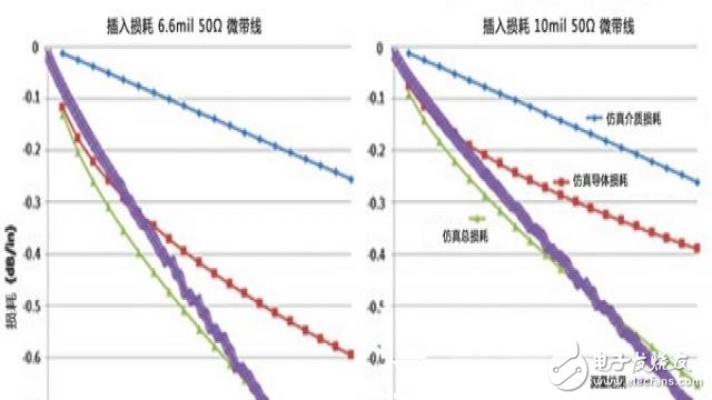
Figure 1. Comparison of 50 ohm microstrip transmission line circuits based on different thickness PCB materials
Measured and simulated results
The curve in Figure 1 contains the measured results and the simulation results. The simulation results were obtained using Rogers' MWI-2010 microwave impedance calculation software. The MWI-2010 software cites the analytical equations in the classic papers in the field of microstrip line modeling. The test data in Figure 1 was obtained by the differential length measurement method of the vector network analyzer. It can be seen from Fig. 1 that the simulation results of the total loss curve are basically consistent with the measured results. As can be seen from the figure, the conductor loss of the thinner circuit (the left curve corresponds to a thickness of 6.6 mil) is the main component of the total insertion loss. As the thickness of the circuit increases (the thickness of the right curve is 10 mils), the dielectric loss and conductor loss tend to be close together, which together constitute the total insertion loss.
The circuit material parameters used in the simulation model and the actual circuit in Figure 1 are: dielectric constant 3.66, loss factor 0.0037, and copper conductor surface roughness 2.8 um RMS. When the surface roughness of the copper foil under the same circuit material is reduced, the conductor loss of the 6.6 mil and 10 mil circuits in Figure 1 is significantly reduced; while the effect is not significant for the 20 mil circuit. Figure 2 shows the test results for two different roughness circuit materials, the Rogers RO4350BTM standard circuit material with high roughness and the Rogers RO4350B LoProTM circuit material with low roughness.
Figure 2 shows the advantages of processing a microstrip line circuit using a smooth copper foil surface substrate. For thinner substrates, the use of smooth copper foil can significantly reduce insertion loss. For a 6.6 mil substrate, the insertion loss is reduced by 0.3 dB at 20 GHz due to smooth copper foil; 0.22 dB at 20 GHz for a 10 mil substrate; and 0.11 dB for a 20 mil substrate.
As shown in Figures 1 and 2, the thinner the circuit substrate, the higher the insertion loss of the circuit. This means that the thinner the circuit will generate more heat when the circuit feeds a certain RF microwave power. In the case of a comprehensive trade-off circuit heating problem, on the one hand, a thinner circuit generates more heat at a high power level than a thick circuit, but on the other hand, a thinner circuit can obtain a more efficient heat flow through the heat sink. Maintain a relatively low temperature.
In order to solve the heating problem of the circuit, the ideal thin circuit should have the following characteristics: low loss factor of circuit material, smooth copper thin surface, low εr and high thermal conductivity. Compared with high εr circuit materials, the conductor width of the same impedance obtained under low εr conditions can be larger, which is beneficial to reduce the conductor loss of the circuit. From the point of view of circuit heat dissipation, for most high-frequency PCB circuit substrates, although it is very poor thermal conductivity with respect to the conductor, the thermal conductivity of the circuit material is still a very important parameter.
A large discussion of the thermal conductivity of circuit substrates has been covered in earlier articles, and this article will cite some of the results and information in earlier articles. For example, both the following equations and Figure 3 are helpful in understanding the influencing factors associated with the thermal performance of PCB circuit materials. In the equation, k is the thermal conductivity (W/m/K), A is the area, TH is the heat source temperature, TC is the cold source temperature, and L is the distance between the heat source and the cold source.
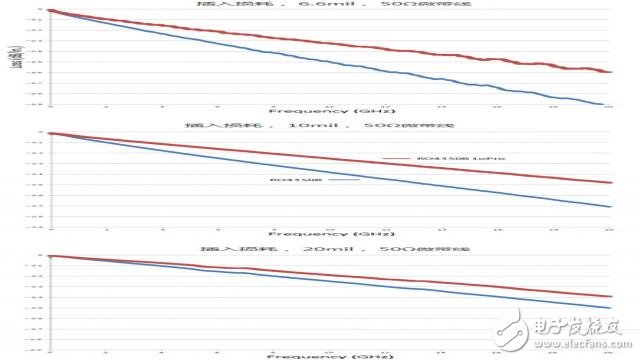
Figure 2. Comparison of microstrip transmission line losses based on different dielectric layer thicknesses and copper conductor roughness
Thermal model
Figure 3 and its equations are a simple representation of the microstrip line circuit thermal model. In the microstrip line circuit, the top conductor layer serves as a signal plane, and the bottom conductor layer serves as a ground plane, and a dielectric layer is filled between the two planes. In the thermal model of Figure 3, the signal plane is assumed to be the heat source and the heat is generated by the signal plane, which has a heat sink and acts as a cold source, and the substrate acts as a thermal conductor to transfer heat from the signal plane to the ground plane. Although the heat generation process of an actual microstrip line circuit is complicated, such a hypothesis is acceptable for a simple thermal model. In fact, the circuit substrate is a poorly thermally conductive conductor. For example, copper, as a good thermal conductor, has a thermal conductivity of 400 W/m/K; while most commercial PCB substrates have thermal densities much less than this, only 0.2 to 0.3 W/m/K.
The heat flow equation explains why a thin circuit (smaller L) can improve heat flow and achieve better heat dissipation at high power levels. At the same time, under high power conditions, high thermal conductivity substrates have higher heat flow and better heat dissipation than low thermal conductivity substrates.
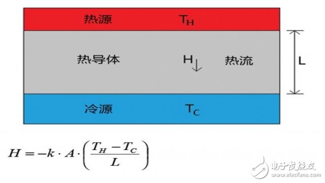
Figure 3. Basic thermal model of a microstrip transmission line circuit, the signal plane is a heat source, and the ground plane with heat sink is a cold source
The power limit of a high frequency PCB circuit depends on the temperature at which the circuit is heated by the power level. The circuit material UL safety certification also obtains the material's Rated Thermal Index (RTI), which is the maximum temperature allowed for the circuit material to operate for a certain period of time without degrading the critical performance of the PCB. When the substrate is fabricated into an actual circuit, some other factors must be considered from the viewpoint of heat treatment. For example, the circuit can also perform a MOT evaluation to measure the maximum temperature allowed by the circuit material for a certain period of time without degrading the critical performance of the PCB. For the same PCB circuit material, the MOT value is always lower than the RTI value.
The RF microwave power of the PCB is limited by the MOT of the circuit and the working environment of the circuit. This power level is acceptable if the circuit power caused by the loaded power does not exceed the MOT of the circuit. Of course, the power applied can cause the circuit to heat up and cause the circuit temperature to exceed the external ambient temperature. When the external temperature is +25 ° C, the heat generated by the loaded RF microwave power will not exceed the MOT. When the external temperature is +50 ° C, the same power level is still applied to the circuit, and the heat generated by the circuit may exceed the MOT and cause problems in the circuit. As analyzed above, the power level of the high frequency PCB circuit depends to some extent on the external working environment.
Influencing factor
In order to better understand the influencing factors related to the thermal performance of the PCB circuit, the 50 ohm microstrip transmission line circuit of the structure of Fig. 1 and Fig. 2 was used for research. Circuits of different thicknesses and different copper roughnesses are machined on the same type of PCB material. In addition, in addition to processing tightly coupled grounded coplanar waveguide microstrip lines on low loss PCB materials, circuits are also processed on high loss PCB materials for evaluation. The input RF microwave power range is 5W to 85W, and all circuits have a return loss of more than 18dB at 3.4GH and a 0.25-inch covered copper plate as the heat sink. The circuit is covered on a heat sink by a COOLSPAN® electrically conductive conductor film with a thermal conductivity of 6 W/m/K.
The infrared imager was used to record the heating of the circuit under certain power conditions. In order to ensure the accuracy of the measurement, the color of the circuit and its surface in the field of view of the infrared imager should be consistent. Using black lacquer as the surface color allows the thermal imager to obtain accurate thermal imaging images. Disadvantageously, the use of black lacquer increases the insertion loss of the transmission line. The increase in insertion loss causes the recorded heat to increase and can be considered as the worst case heat. In addition, since the ground-signal line-ground area of ​​the coplanar waveguide covers the black lacquer and the current density of the area is large, the influence on the insertion loss (temperature rise) of the grounded coplanar waveguide is greater than that of the microstrip line circuit.
Table 1 shows the circuit structure, material type and characteristic parameters, insertion loss and temperature rise results of different circuits. This table provides a wealth of information for comparing the thermal effects of different circuit materials. For example, the thermal effects of circuits using different copper foil roughness based on the same circuit substrate can be compared from the table, the No. 3 circuit uses a rough copper foil, and the No. 4 circuit uses a smooth copper foil. As expected, the circuit on the smooth copper foil surface has a lower insertion loss than the circuit on the rough copper foil surface, so the temperature rise of the No. 4 circuit is also smaller.
Table 1. Temperature rise of circuits based on different structures and materials under the same power conditions
Comparing the No. 1 circuit and the No. 3 circuit, it can be found that the change in the thickness of the PCB material causes a difference in the rising temperature. These two circuits have the same material type and copper roughness except for the difference in PCB thickness. The No. 1 circuit is thinner than the No. 3 circuit, and its insertion loss is also higher than that of the No. 3 circuit. As mentioned earlier, when the circuit applies sufficient RF microwave power, the higher the insertion loss, the more heat is generated. However, as shown in Table 1, the rise temperature of the thinner No. 1 circuit is actually lower than that of the thicker No. 3 circuit. This is because the circuit No. 1 has a shorter heat flow path L as shown in FIG.
Comparing the No. 1 circuit and the No. 2 circuit, it can be found that the materials used in the circuit are identical, but the circuit design of the two is different. Circuit No. 2 is a coplanar waveguide circuit that is tightly coupled and has a plated through hole (PTH) near the edge of the coplanar ground-signal line. A comparison of the structure of the microstrip transmission line and the coplanar waveguide transmission line is shown in FIG.
Insertion loss
The coplanar waveguide circuit with tightly coupled structure has better heat dissipation performance than the microstrip line circuit. The center signal conductor of the coplanar waveguide circuit (No. 2 circuit) has a pitch of 5 mils between the center signal conductor and the adjacent ground conductor, and a row of ground vias are distributed at the edge of the ground conductor. These vias are plated copper holes that act as heat transfer paths to effectively transfer heat from the signal plane to the ground plane. As shown in Table 1, the difference in insertion loss between the No. 1 microstrip line circuit and the No. 2 grounded coplanar waveguide circuit is very significant. Since both circuits are fabricated on the same thickness of material, the higher the insertion loss of the circuit means the more heat is generated. Although the grounded coplanar waveguide circuit generates more heat than the microstrip line circuit, the heat dissipation effect of the ground vias does not cause much difference between the temperature rises of the two.
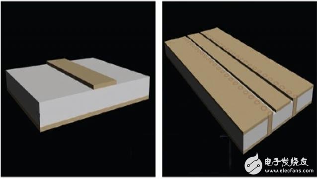
Figure 4. Transmission line circuit for PCB thermal effect study (a) microstrip line structure (b) grounded coplanar waveguide structure corresponding to circuit No. 2
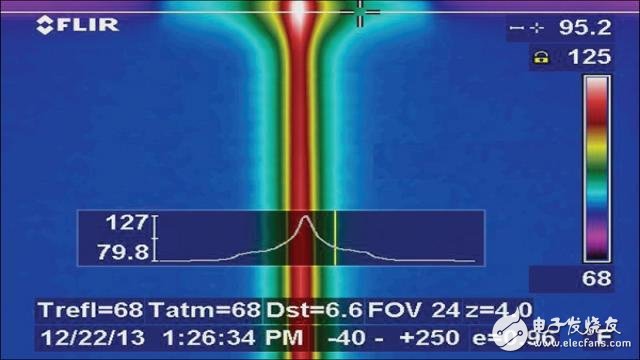
Figure 5. Microstrip transmission line overlooking the thermal imaging image, the apex corresponds to the heat at the signal feed point
Finally, comparing the No. 3 circuit and the No. 5 circuit in Table 1, it can be found that except for the PCB thickness of 20 mil, many other parameters are different. Circuit 5 is based on a low cost FR-4 circuit material that is rarely used in the microwave band. The insertion loss of circuit No. 5 is significantly higher than that of circuit No. 3. In addition, Circuit 5 also has many shortcomings in thermal performance, including high loss factor, low thermal conductivity, and high εr. For a 50 ohm transmission line, a high εr means that the wire width is narrowed, and the conductor loss of the circuit No. 5 is higher than that of the low εr circuit No. 3.
For any circuit thermal study, signal feed is often a critical point in the circuit because it is desirable to transfer RF power from the input port to the circuit under test as efficiently as possible. In this study, all experiments used a good 3.5mm termination connector from Southwest Microwave(). Although the circuit is optimized for good signal feed, there is always a certain amount of energy loss near the signal feed zone, which results in higher heat in the feed zone. Since the firing joint is a good thermal conductor, some of the heat can be conducted through the joint to the heat sink. Under high power conditions, as shown by thermal imaging, the temperature of the circuit signal feed region is higher than the temperature of the body portion of the microstrip circuit. Figure 5 corresponds to a circuit thermographic image of the above case, which circuit does not belong to the circuit listed in Table 1.
Figure 5 is a thermographic image of a 12 mil thick 50 ohm microstrip transmission line circuit. The insertion loss of this circuit after spraying black paint is 0.23 dB/in. The maximum temperature of the circuit signal feed zone is +127 °F, while the maximum temperature of the main part of the circuit is +119 °F. Since the signal feed zone has more heat sinks than the main body of the circuit, the temperature difference between the two measurements is not large, but the difference is still worthy of attention.
in conclusion
From the perspective of heat control, different factors of insertion loss, simple thermal model and some main circuit material parameters are analyzed to help understand the thermal effects of PCB circuits under high power RF microwave signal conditions. In general, relatively thin circuit materials, high thermal conductivity, smooth copper foil surface, low loss factor, etc. are all beneficial to reduce the heating effect of PCB circuits under high power RF microwave signal conditions.
Cold Cathode Uv Lamp,Ceramic Cold Cathode Uv Lamp,Portable Cold Cathode Uv Lamp,Home Cold Cathode Uv Lamp
t-smartlight , https://www.t-smartlight.com