Virtex-5 drives the development of ultra-wideband communications and ranging
Since the U.S. Federal Communications Commission (FCC) approved the unlicensed use of ultra-wideband (UWB) technology in 2002, most commercial applications have relied on frequency domain modulation techniques like OFDM for high-speed data transmission. However, UWB’s unique capabilities also make it ideal for nanosecond-level pulse-based communication systems known as impulse radio (IR). These systems transmit information by modulating pulse characteristics such as position or amplitude, and they can achieve centimeter-level precision in distance measurement by analyzing the time-of-flight of pulses. This has opened up new possibilities for location-aware applications across various fields, including logistics (e.g., package tracking), manufacturing, search and rescue (like firefighter positioning), and smart guidance systems.
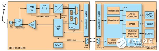
Figure 1: The system consists of a non-customized Xilinx ML506 board connected to a custom UWB daughter board.
In Europe, the second phase of the PULSERS project is an industry-led initiative involving 30 major academic and industrial partners. The goal is to develop an IR-UWB communication and ranging system capable of achieving a data rate of several megabits per second with a range accuracy of 4 cm. The system is composed of identical autonomous nodes that can communicate with each other and calculate distances. Each node is equipped with a custom UWB daughter board connected to a standard Xilinx ML506 development board (see Figure 1). The powerful Virtex-5 SXT architecture, combined with the flexibility of the MicroBlaze soft processor, allows us to implement the entire baseband signal chain and advanced system layers within a single FPGA.
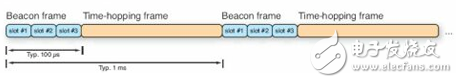
Figure 2: A periodic beacon frame consisting of three beacon slots is interspersed between time-hopping frames.
IR-UWB Communication and Ranging
The system uses simple pulse-position modulation (PPM) to encode data, supporting four possible time shifts (4-PPM), where each pulse carries two bits of information. As shown in Figure 2, pulses are grouped into frames and transmitted in a structured pattern of beacon and time-hopping frames. Each beacon frame includes three identical slots that can be used for ranging or communication. Initially, we planned to use time-hopping frames for high-speed data transmission, but due to technical challenges, all current data is now transmitted exclusively through beacon frames.
For ranging, we employ a two-way time-of-flight technique. This involves measuring the delay between sending a ranging request and receiving a response from a remote node. Typically, the ranging request is sent in beacon slot 1, and the response is returned in beacon slot 3, giving the remote node approximately 33 microseconds (beacon slot 2) to process and respond.
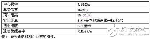
Table 1: Characteristics of UWB communication and ranging systems.
System Structure
The UWB daughter boards used in this project were designed using IHP’s 0.25 micron SiGe:C BiCMOS technology, featuring pulse transmitters and non-coherent receiver ASICs. As shown in Figure 3, the transmitter ASIC generates UWB pulses and can modulate both their amplitude and position. It includes a 3.84 GHz counter for precise scheduling of pulse transmission and reception timing.
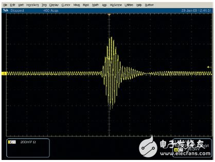
Figure 3: The UWB pulse consists of a 7.68 GHz carrier and a Gaussian envelope.
The receiver ASIC splits the incoming signal into two branches. The first branch, with a narrower bandwidth (120 MHz), is primarily used for communication and less accurate timing, while the second branch, with full pulse bandwidth (750 MHz), provides precise timing. A high-speed comparator detects the incoming pulse, triggering the readout of the 3.84 GHz counter inside the transmitter ASIC. This enables pulse arrival times to be measured at a resolution of 260 picoseconds, corresponding to a spatial resolution of about 8 cm.
The daughter board communicates with the baseband module in the Virtex-5 FPGA via two 120 MHz data buses. One bus handles ADC samples for communication, while the other transmits high-resolution time stamps for received pulses. Both buses pass through an XC95144XV CPLD, which serves as a useful debugging tool. By configuring the CPLD to output pseudo-random patterns, we can verify the integrity of the bus lines and adjust timing inputs in the FPGA. Without knowing the data sequence, verifying the bus would be significantly more challenging.
C194 Copper IC Lead Frame,Copper IC Lead Frame,Smooth IC Lead Frame
SHAOXING HUALI ELECTRONICS CO., LTD. , https://www.cnsxhuali.com