The concept and key factors of embedded vision
Author: Aaron Behman, Adam Taylor
Vision-based systems have become very common in many industries and applications. In fact, many of us carry an embedded vision system every day, such as in our smart phones. These smart devices can not only capture images and record video, but also perform augmented reality applications, which demonstrate how embedded vision technology is widely accepted.
The increase in processing power, memory density, and system integration has contributed to the growth of embedded vision in traditional and emerging applications (examples shown in Figure 1). This also makes embedded vision widely accepted in the consumer, industry and government sectors, and will therefore achieve significant growth within a decade. Table 1 lists some of the high-growth areas of embedded vision, some of which are obvious and some are not.
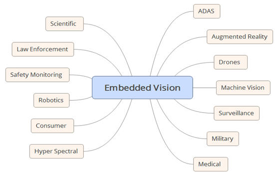
Figure 1 Common embedded vision applications.
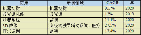
Table 1 Expected embedded high growth areas
What is embedded vision?
The embedded vision system includes the entire signal chain that receives light from the selected imaging sensor to the system output. System output refers to processed or unprocessed images or information extracted from images and provided to downstream systems. Of course, embedded system architects are responsible for ensuring end-to-end performance based on system requirements.
For this reason, embedded vision system architects need to be familiar with various concepts and technologies related to sensors and post-processing systems. This article serves as a high-level introductory manual designed to give readers a basic understanding of these technologies and concepts.
You first need to be familiar with the electromagnetic spectrum and the spectral domain that you want the system to operate. The human eye can only see the spectrum between 390 nm (blue light) and 700 nm (red light) wavelengths, which is commonly referred to as the visible light spectrum; imaging equipment can capture wider wavelength images, including X-ray, ultraviolet, infrared and visible spectrum.
In the near-infrared spectrum and the following range, we can use charge-coupled device (CCD) or CMOS (complementary metal oxide semiconductor) image sensors (CIS); to the infrared spectral range, the use of dedicated infrared detectors. Particular reasons for the need for dedicated sensors in the infrared spectral range lie in the excitation energy required by the chip imager (such as CCD or CIS). These devices typically require 1eV of photon energy to excite an electron, whereas in the infrared range the photon energy is between 1.7eV and 1.24meV, so the infrared imager should be based on HgCdTe or InSb. These devices require lower excitation energy and are often used in conjunction with CMOS readout ICs (ROICs) to control and read sensors.
The two most common detector technologies are CCD and CIS.
• Charge-coupled devices are considered analog devices, so integration into digital systems requires the use of an off-chip ADC and clock generation at the desired analog voltage level. Each pixel stores the charge generated by the photons. In most cases, the pixels are arranged in a 2D array, forming multiple rows, each containing multiple pixels. When the CCD is read out, each row is transferred in parallel to the read register by row transfer, and each row is read out serially by reading out the register. During this register readout, the charge is converted to voltage.
• CMOS imaging sensors enable tighter integration and integrate the ADC, bias, and drive circuitry on the same chip. This greatly reduces system integration requirements and also increases the complexity of the CIS design. At the heart of the CIS is an active pixel sensor (APS), where each pixel contains both a photodiode and a sense amplifier. Therefore, unlike a CCD, a CIS can read any pixel address in an array.
Although most embedded vision uses CIS devices, CCDs are still used in high-end scientific applications that focus on performance. The main points of this article apply to both imaging technologies.
Sensor considerations
Choosing the right sensor requires understanding of the system requirements and must be considered from several aspects of the device.
The first requirement is that we must determine the required resolution, which is how many pixels per line, and how many lines the detector needs. The final application is decisive. For example, astronomical applications for scientific research may require high resolution 2D devices, while industrial inspection imaging may only require line scan solutions.
• Line scan devices contain a single line (sometimes a few lines) of pixels in the X direction. If the Y-direction image is generated by the movement of the camera or the target, such devices are generally used. They are used for inspection or in the field of optical character recognition (OCR). Some areas require the use of time-domain-integrated (TDI) line scan sensors. This type of sensor contains multiple lines in the X direction. As the target moves, the pixel values ​​also move from one to the next, enabling more sensitive detection as the charge is integrated over time. However, TDI needs to be synchronized between the line transfer and the target move to prevent blurring and image defects. Since only a few lines need to be read out, the frame rate can be very high.
• 2D arrays contain multiple rows with multiple pixels per row. Array size is a factor that determines the maximum frame rate of the sensor. In general, 2D devices read out multiple pixels in parallel in order to achieve higher frame rates. 2D devices can also perform window operations (sometimes referred to as areas of interest) that read only specific areas of interest for higher frame rates. This type of device can be used in many fields, and the information is included in 2D images such as advanced driver assistance systems (ADAS), surveillance or scientific research.
After determining the imager format and the desired resolution, we must also consider the pixel pitch. The pixel pitch defines the size of the pixel and determines how much incident photon energy can be collected. Therefore, a smaller pixel pitch means that less charge is collected during the integration period (the time the sensor is exposed in the image). If the pixel pitch is small, it means that the capture image requires a longer integration time, which affects the ability of the sensor to capture fast-moving images and reduce the low light photo performance.
After determining the sensor format, we must consider which technology to use, CCD, CMOS or more specialized technologies. The important parameter here is the quantum efficiency (QE); this parameter is the efficiency of the device to generate electrons through photons. In general, we want to achieve as high a QE as possible in the useful spectrum, which is also important for low-light applications. There are three factors that affect the device QE: absorption, reflection, and transmission. One of the main causes of QE reduction is the device structure. The device structure may cause the pixels to be shielded by the circuitry in the sensor, such as metal lines or polysilicon gate circuits. These structures absorb or reflect photons, which lowers QE, so choose the sensor.
• Front-illuminated - For this type of device, photons illuminate the front of the device in the manner described above. Pixels may be obscured and QE reduced accordingly.
• Back-illuminated - These devices are post-processed to thin the back of the device so that it receives light behind and is not blocked by other design elements. Thin back-illuminated devices achieve the best QE.
We must also consider the noise allowed in the image sensor; there are three main aspects to consider.
• Device noise - This is temporary in nature and includes scattered noise and noise from the output amplifier and reset circuitry.
• Fixed Pattern Noise (FPN) - Spatially distributed, caused by different responses of pixels at the same light intensity. FPN is usually caused by different offsets and gain responses for each pixel; the offset part is often called dark signal response non-uniformity (DSNU) and the gain part is called image response non-uniformity (PRNU). There are several ways to compensate for FPN. The most common method is the correlated double sampling of the output signal.
• Dark current - This is caused by thermal noise in the image sensor, even in the absence of light. The effect of the dark signal on the final image quality depends on the frame rate; the effect is not significant at higher frame rates, however, the effect can be significant as the frame rate decreases (eg, for scientific applications). Since the dark current is temperature dependent, it is common practice to use a cooling device (such as Peltier) to reduce the operating temperature of the imaging device in the event that the dark current needs to be reduced.
After understanding the imager's noise pattern, we can determine how much signal-to-noise ratio (SNR) can be achieved.
After determining the noise performance of the device, the required dynamic range of the image sensor can be determined. The dynamic range represents the ability of the sensor to capture images with a wide range of illumination in units of dB or as a ratio. This means that the image contains both high and dark areas.
The actual dynamic range of the sensor is determined by the full well capacity of the pixel, which is the amount of electrons that can be carried before the pixel is saturated. Dividing the capacity by the readout noise can easily convert the ratio to a value in dB.
(potential well capacity e-)/(reading noise e-)
Normally, the photon conversion curve test method is used to determine the dynamic range, and the relationship between noise and capacity is plotted.
If the device has a digital output, this value can be calculated using the output bit number using the following formula.
Dynamic range (dB) = 20 Log10 (2^ bus width)
However, this does not guarantee that the device can achieve such a dynamic range; it merely specifies the potential range that the bus width can represent without considering the sensor performance factor.
The IO standard is also important not only for outputting pixel data but also for outputting commands and control interfaces. This is related to the frame rate. For example, the LVCMOS interface is not suitable for high frame rate applications, but it can be used for simple surveillance cameras. With the increase in frame rate, resolution, and bits per pixel, the trend for imaging devices is moving toward dedicated high-speed serial links using LVDS series or SERDES technology.
Now that we have introduced several important aspects of image sensors, another factor that has not yet been considered is whether the imager is a color or monochrome sensor. Whichever you choose, it depends on the application.
• Color Sensors—Bell graphics need to be used on each pixel, alternately changing red and green on a line, alternating blue and green on the next line (green is used much more because the human eye is more sensitive to the wavelength of the green color). This means that the received photons are filtered so that each pixel only receives photons with the desired wavelength. We can post-process the image by surrounding the pixels with different colors to reconstruct the color on each pixel to determine the pixel color without degrading the image resolution. Color sensors complicate the image processing chain needed to reconstruct and output images. Bell's graphics do lead to a decrease in resolution, but they are not as bad as they were supposed to be, usually by 20%.
• Monochrome — Because there is no Bell pattern on the image array, each pixel can receive all photons. This increases image sensitivity and makes image reading easier because there is no demosaic effect required for color reconstruction.
After choosing we decided to use CIS devices, in fact these are complex specialized system-on-chips. Therefore, we must also consider the following issues regarding readout mode and integration time.
• Integration time - This is the exposure time of the pixel before reading. On a relatively simple CCD system, it is necessary to approach the electronic device to perform this timing outside the device. However, for CIS devices, the integration time can be configured by registers through the command interface, and then the CIS device accurately performs the integration time for the two commonly used readout modes.
• Global Shutter Mode - In this mode, all pixels receive light at the same time and then read out. In this mode, readout noise is increased because all pixels are read at the same time. This mode is suitable for taking snapshots of fast moving objects.
• Rolling Shutter Mode — In this mode, progressive exposure and reading are performed. This mode reads less noise, however, it is not as good as the global shutter mode in capturing fast moving objects.
System Development
After choosing the right sensor, many challenges need to be considered and solved during system development.
In addition to technical challenges, there are also time pressures in the development of the system to ensure that products are delivered to the market within a given time frame. Based on time constraints, we need to focus on what activities in the development process can achieve added value and then make the right choices to distinguish which parts should be developed (value-added activities) and which parts can be purchased for commercial off-the-shelf products (COTS) or points. Package out. Focusing on value-added activities and leveraging IP modules at the hardware, software, and FPGA levels is one of the key contributing factors to meeting time-to-market requirements.
In addition to time-to-market requirements, size, weight, power, and cost (SWAP-C) requirements are often considered in the development of embedded vision systems. Which kind of requirements dominates depends on the specific application area. For example, handheld devices are more rigorous in terms of power consumption than driver assistance systems. However, for advanced driver assistance systems, the cost of the solution becomes the dominant factor due to the production of millions of units.
To achieve good results in terms of size, weight, power consumption, and cost, tighter system integration should be implemented in sensors and processing systems, that is, using fewer but more powerful integrated components.
Each application area has different value-added points and different size, weight, power consumption and cost considerations, so almost all embedded vision systems require us to implement a so-called image processing pipeline. This pipeline can interface with selected sensors and perform the required operations to generate images suitable for further processing or transmission directly over the network. The basic image processing pipeline includes:
• Camera Interface - Receives raw images from the sensor
• Color Filter Array - Rebuild Pixel Colors
• Color space conversion - Convert to the correct color space for the codec.
• Output Format - Interface with output media
The algorithm is executed and applied to the received image in the image processing pipeline. The algorithms used will be different depending on the application being implemented; however, there are some commonly used image processing algorithms that can be used to improve contrast, detect characteristics, targets or motion in the image, or correct blurred images.
These algorithms should be developed in a framework so that we can bring products to market in the shortest possible time and encourage reuse, reducing non-repetitive and repetitive engineering costs. There are several ready-made frameworks that we can consider using.
• OpenVX - an open source application for developing image processing applications.
• OpenCV - open source computer vision, multiple libraries for real-time computer vision, based on C/C++
• OpenCL — A C++-based open source computer language used to develop common parallel processing applications in devices such as GPUs and FPGAs.
• SDSoC—A Xilinx design environment that enables developers to initially implement algorithms written in C/C++ on an ARM processing system in Zynq or UltraScale+ MPSoC devices, analyze code library features to identify performance bottlenecks, and then These bottlenecks are converted to hardware-backed IP cores using Xilinx high-level synthesis capabilities and run in the programmable logic (PL) portion of the device.
When using FPGAs or All Programmable SoC schemes, these frameworks can be used in conjunction with HLS to efficiently develop embedded vision applications and quickly demonstrate them in closed loop with hardware.
After the image goes through the processing pipeline, the data output from the system is also very important. We have three options.
• Output images to the monitor using standards such as video graphics array (VGA), high-definition multimedia interface (HDMI), serial digital interface (SDI), or DisplayPort. Many electric cars use touch screens to control and configure the system.
• Transfer images or information extracted from images to another system that uses images or extracted information like cloud processing applications
• Store images on non-volatile memory for later access.
For most of the methods, after the imaging chain is completed, we need to determine the image format for use. At this point, we need to decide whether to encode images using industry-standard image/video compression algorithms such as H.264 (MPEG-4 Part 10 Advanced Video Coding) or H.265 (High Efficiency Video Coding). These implementations are often called As a codec. Codecs can increase the efficiency of the use of communications and network bandwidth, or reduce the storage space required to achieve high fidelity, because the coding usually has large distortion. If distortion is unacceptable due to the use of a codec, you can also send and store the image in its original format or encode it in a lossless format.
The color space used by most codecs is different from the color space output by the image sensor (provided the system uses a color device). The color space commonly used in embedded vision is:
• Red, Green, Blue - Contains RGB information as the output of the image sensor, often used as the output of a simple interface such as VGA
• YUV - Contains luminance (Y) and chrominance (U and V) used for most codecs and some display standards. The commonly used YUV formats are YUV4:4:4 and YUV4:2:2. The difference between the two formats is that in the 4:4:4 format, each pixel is represented by 8 bits, resulting in 24 bits of pixels. In the 4:2:2 format, the U and V values ​​are shared between pixels, resulting in 16-bit pixels, which saves storage space.
Another decision that has a big impact on the image processing chain and SWAP-C is where most of the image processing chain should be implemented:
• On the edge, ie within the embedded vision system. This will increase the system's power consumption and processing/storage requirements, but it will enable faster response. The edge processing will be dominant in most embedded applications (eg advanced driver assistance, machine vision, etc.).
• In the cloud, this requires embedded vision systems to capture images and use web technologies to send images to the cloud. Typical applications that can be processed in the cloud include medical imaging or scientific applications. In such applications, the processing is very intensive and does not require real-time results.
To implement the processing chain, the processing core at the heart of the embedded vision system must not only control the selected image sensor, but also receive and implement image processing pipelines, and send images to selected displays via designated network infrastructures. Given these stringent requirements, FPGAs are often chosen, or more and more cases require the use of All Programmable system-on-chips, such as Zynq devices.
The Zynq device combines two high-performance ARM A9 processors with an FPGA architecture. This allows the processing system (PS) to be used to communicate with the host system through GigE, PCIe, or CAN interfaces while performing general management and day-to-day affairs of the system. The other half of the device, Programmable Logic (PL), can be used to receive and process images, taking full advantage of the parallel processing features of the FPGA fabric. If you require the transfer of images through the network infrastructure, you can use the Direct Memory Access (DMA) controller in Zynq to efficiently move image data from the PL to the PS DDR memory. The image is in the PS DDR memory and can be further accessed using the DMA controller of the selected transmission medium.
Of course, the high-performance A9 processor can provide further processing once the image is in PS DDR. The Zynq architecture also features the ability to move processed images from PS DDR back to the image pipeline in the PL.
Sensor fusion
Many embedded vision systems also require the ability to integrate more sensor data to better sense the environment. This includes the use of many sensors of the same type (convergence of sensors of the same type) to expand the field of view, such as panoramic functions of advanced driver assistance systems; or integrate multiple different types of sensors (heterogeneous sensor fusion) to provide visual content that cannot be seen in the visible spectrum. For example, infrared information is superimposed on conventional image sensor data.
In many cases, the output of the embedded vision application needs to be fused with other sensor data so that the resulting image contains information from multiple different sensors. The simplest application of sensor fusion is to combine different spectral images, such as visible light and infrared light, to achieve better night vision effects.
Another, more sophisticated use of sensor fusion is to fuse the imaging system, Global Navigation Satellite System (GNSS), digital map information, and other sensors operating at different wavelengths (such as radar) to determine the relative position of another car. To achieve collision avoidance.
Because of the need to fuse different systems together and extract information, the sensor fusion requirements for the processor can be very high. All Programmable system-on-chip solutions can interface with multiple sensors, process information in parallel, and increase data throughput, resulting in a number of significant advantages.
in conclusion
Embedded vision has become very common, and its market penetration and application range will only increase in the next decade.
At the sensor and system level, there are several factors that must be considered. There are multiple technologies, frameworks, and devices that can be used to implement an embedded vision system.
Silent Type Diesel Generator,Soundproof Diesel Generator,Diesel Generator Set,Pump Generator
Jiangsu Vantek Power Machinery Co., Ltd , https://www.vantekpower.com